| john@email.johncon.com |
| http://www.johncon.com/john/ |
|
|
|
||
DIY Negative Dry Etch PCB Fabrication |
|||
Home | John | Connie | Publications | Software | Correspondence | NtropiX | NdustriX | NformatiX | NdeX | Thanks
|
This is the documentation for the method the author uses for DIY quick turn prototype printed circuit boards, (PCBs.) The documentation to the steps required is quite granular, with complete documentation, and the rationale for each step is presented with the exact equipment and materials used, along with measurements for optimizing and certifying the process. The process is based on the industry standard process used by commercial PCB vendors. The artwork for the analysis and certification procedure, 10x10.tar.gz, is available as a tape archive. The idea being that the process could be easily replicated and functions as a base line known workable process, complete with certification and quality control methodology. The exact equipment, materials and vendors used, (as of 2017,) are listed to avoid availability issues. The author is not affiliated in any way with any vendor, manufacturer, or distributor of equipment, components, parts, materials, or sites mentioned in this document. Artwork generation for the PCB, (Rationale):
Cleaning the PCB, (Rationale):
Applying the dry film to the PCB, (Rationale):
Laminating the dry film to the PCB, (Rationale):
Assembling the print frame for the PCB, (Rationale):
Exposing the PCB, (Rationale):
Developing the PCB, (Rationale, Alternatives):
The spent developer solution will be saved for stripping the photoresist from the PCB, below. Rinsing the PCB, (Rationale):The PCB should be removed from the developer solution and rinsed in a container of luke warm tap water, (~98F, baby bottle temperature test,) by scrubbing the PCB, vigorously, with a microfiber cloth using significant finger pressure, for 24 to 30 seconds, (2 minutes 30 seconds to 4 minutes if the alternative developer process of floating the PCB in the developer solution is used.) Etching the PCB, (Rationale):The PCB should be placed in a 1 liter polypropylene, TashiBox Plastic Food Container / Food Storage / Soup Container with Lids, 32 Ounce - Set of 24 with a 2:1 H202 3%:HCL 31% new etching solution, for about 5 minutes, The 1 liter etch solution in the polypropylene container is placed in a 6 qt. plastic tray of very hot tap water, (~ 150F,) for about 15 minutes prior to etching the PCB to raise the temperature of the etch solution. The 3% H2O2 is available at the local drugstore, (usually used as an antiseptic and/or mouthwash-be careful NOT TO USE 30% H2O2,) and the 31% HCL is available at the local home improvement store in the swimming pool chemicals department. For HCL 14.5%, and, H2O2 3%, use 2 3/4 cups = 660 ml of HCL 14.5% and 1 1/2 cups = 360 ml of H2O2 3%. Drilling the PCB, (Rationale):As mentioned, above, the pads and vias for manually assembled PCBs should be as large as possible, (limited by the PDIP package,) with a minimum drill size of 0.9mm = 35 mils, and, 20 mil annular ring, (i.e., 20 mils of copper around component holes,) for a total pad diameter of 75 mils, and a clearance for the PDIP package of 20 mils between pads. For negative resist, there is a "drill helper" center punch indentation in the center of each copper pad, (and photoresist,) to assist targeting the drill bit for manually drilled component holes in the PCB. Striping the PCB, (Rationale):The PCB should be placed in the spent developer solution after heating the spent developer to 125F in a microwave, (for about 1 minute-it contains about as much fluid as a cup of coffee.) Stripping the photoresist takes about 5 minutes. Soldering the PCB, (Rationale):The soldering iron temperature for assembling components on the PCB should be set to about 350C = 662F, (but could be as low as 315C = 600F, to as high as 388C = 750F, depending on user preference,) for through hole PCB components. The solder should be 63/37 tin/lead, 1.1% flux, 0.031" = 0.8 mm. Finishing the PCB:After assembly/soldering, the flux can be removed with 91% isopropyl alcohol, (available from any pharmacy,) and an acid brush. If durability of the PCB is required, (i.e., function for years or decades,) coating the copper side of the PCB with clear acrylic spray, or fast drying polyurethane spray, (both available from home improvement stores in the paint department,) will avoid tarnishing and oxidation of the copper surface. Cost analysis for the PCB process:The complete bill of materials to duplicate the above process, from scratch is US $198.14, (as of 2017, and much of that cost is not necessary unless one wants to do additional process development; to only make PCBs, this cost can be reduced by approximately 75%,) which includes enough expendables for 50 ea. 100mm X 70 mm FR1 PCBs. The incremental cost per PCB after the bill of materials is about US $0.54 in expendables, including the FR1 PCB. (The variance in cost is the H2O2 3% followed by the cost of HCL 31%.) The fast process, (scrubbing in the developer and rinse,) takes about 12 minutes and 19 seconds process time, (plus the time it takes to clean the PCB, apply the dry film, assemble the print frame, and run the PCB through the laminator, which depends on how fast one works-typically, an additional 3 minutes-but has been done in under 1 minute on a bet.) Call it about 15 minutes to stripped PCB ready to drill and solder. Quality Assurance/Certification for the PCB Process:The process parameters for exposure and development of a PCB have been determined. The parameters interact, (i.e., like under exposure, and over development will sometimes work.) To determine that both processes are optimum, and optimum together, test artwork must be generated.
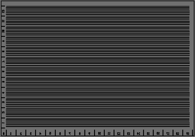
Figure I. Test Artwork MatrixFigure I is a plot of the test artwork for the matrix PCB. The archive for the circuit, 10x10.tar.gz, is available. The idea is that a piece of Rubylith will be placed over the artwork in the print frame, and slid down a half of a centimeter every ten seconds during exposure to vary the exposure from 0 to 200 seconds with 5 inches between the 150 X SMD 5050 UV LEDs and the PCB. The Rubylith is slid down from the top short edge, to the bottom short edge. Then, the exposed PCB is developed, by turning the PCB vertically in the developer container, (long edge down,) and adding a half of a centimeter of developer solution every minute, for a developer time of 0 to 10 minutes. The PCB will look like a matrix, (like a spread sheet,) of exposure time vs. developer time, and we look for the longest, narrowest, metal run and clearance as a parameter. The artwork has a 6 mil metal width, and 6 mil clearance, as the narrowest line dimension.
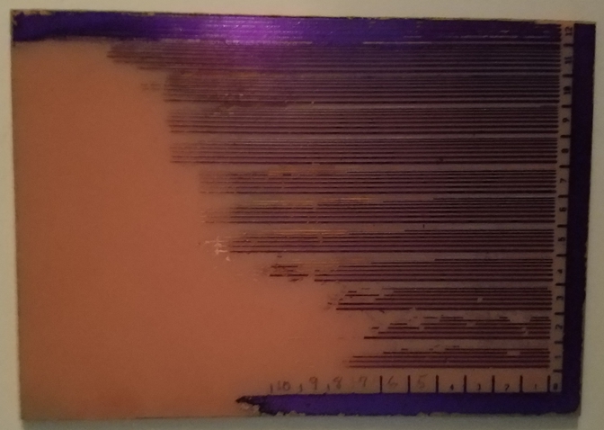
Figure II.Figure II is photograph of the matrix PCB. As oriented, the left side of the PCB is under exposed. The right side of the PCB is over exposed. The bottom of the PCB is over developed. The top of the PCB is under developed. The best lithography, with 5 inches between the 150 X SMD 5050 UV LEDs and the PCB, occurs at an exposure time of about 4 minutes and a developer time of about 4 minutes-the 6 mil metal width and clearance is about 2 cm long in the photograph. This is in reasonable agreement with the original exposure time at 8.5" of 11 minutes, (the actual measurement made in the "Exposing the PCB, (Rationale)" Section was 9 to 13 minutes, probably closer to 9.) The developer time of 4 minutes is in reasonable agreement with the original developer time of 5 to 8 minutes, (the actual measurment made in the "Developing the PCB, (Rationale)" Section. And, finally, a test PCB.
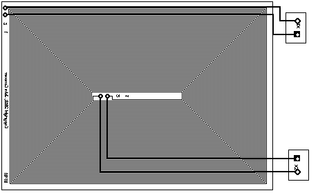
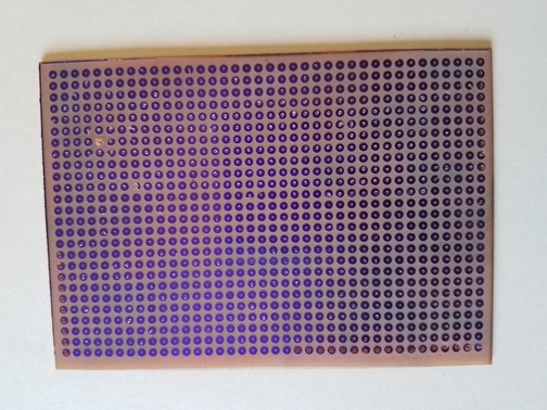
Figure III. "10x10.png"Figure III is a plot of the test PCB, with 10 mil line width, and 10 mil spacing. It is a rectangular spiral of 2 lines, (think of an extension cord, coiled up.) Bridging and opens can be tested with an Ohm meter, (i.e., pins 1-1 should be a short, as should pins 2-2, but pins 1-2 and 2-1 should be open.) The circuit is about 10cm X 7cm, and the total run length is about 40 feet, (20 feet for each of the two lines.) The archive for the circuit, 10x10.tar.gz, is available.
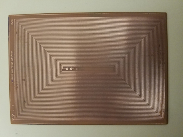
Figure IV. 10x10 PCBFigure IV is a photograph of the test PCB, with 10 mil line width, and 10 mil spacing. It is a rectangular spiral of 2 lines, (think of an extension cord, coiled up.) Bridging and opens can be tested with an Ohm meter, (i.e., pins 1-1 should be a short, as should pins 2-2, but pins 1-2 and 2-1 should be open.) The circuit is about 10cm X 7cm, and the total run length is about 40 feet, (20 feet for each of the two lines.) The smudging is due to handling during testing, photographing, etc. The archive for the circuit, 10x10.tar.gz, is available. A continuity test was done on the 4 pins of 10x10:
A series of 6 micro-photographs to evaluate the PCB process, made with a 100X Optical Zoom Microscope XFox Mobile Phone Microscope with Bright LED Lamp and Universal Clamp for iPhone6/6plus/5c/5s/4/4s Samsung Galaxy S6/S5/S4/Note 4/3/2 etc., and a cell phone are below. The order is the artwork, (3 photographs, left long vertical runs, top short horizontal runs, followed by a corner, with the PCB nomenclature at the bottom,) followed by the PCB photographs in approximately the same area, and the same order.
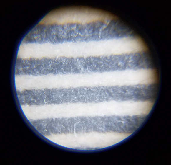
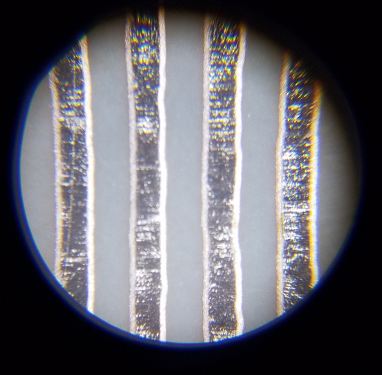
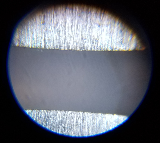
Figure V. 10x10 PCB Artwork, Verticle RunsFigure V is a photograph of the test PCB artwork, verticle runs. The drawn metal width is 10 mils, and the clearance is 10 mils. The produced metal width is 9.4 mils, the clearance is 10.6 mils.
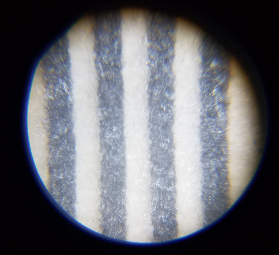
Figure VI. 10x10 PCB Artwork, Horizontal RunsFigure VI is a photograph of the test PCB Artwork, horizontal runs. The drawn metal width is 10 mils, and the clearance is 10 mils. The produced metal width is 10 mils, the clearance is 10 mils.
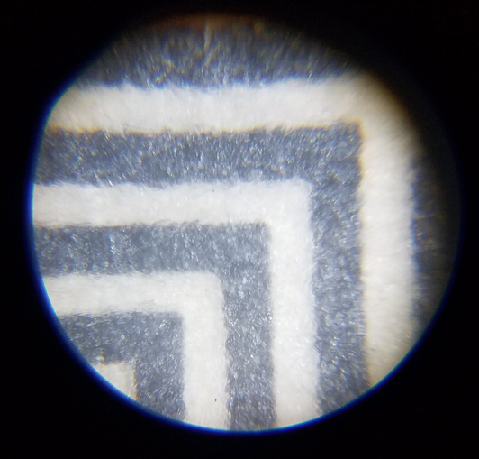
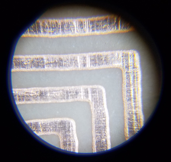
Figure VII. 10x10 PCB Artwork, Corner RunsFigure VII is a photograph of the test PCB artwork, corner runs.
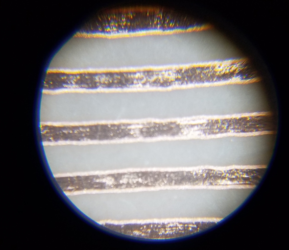
Figure VIII. 10x10 PCB, Verticle RunsFigure VIII is a photograph of the test PCB, verticle runs. The drawn metal width is 10 mils, and the clearance is 10 mils. The produced metal width is 8.5 mils, the clearance is 11.5 mils.
Figure IX. 10x10 PCB, Horizontal RunsFigure IX is a photograph of the test PCB, horizontal runs. The drawn metal width is 10 mils, and the clearance is 10 mils. The produced metal width is 8.5 mils, the clearance is 11.5 mils.
Figure X. 10x10 PCB, Corner RunsFigure X is a photograph of the test PCB, corner runs Artwork generation for the PCB, Rationale:3M has issued a Product Discontinuation for their transparency business. An investigation into alternative media yielded:
The minimum DIY line lithography should support Quad Flat Package geometries, meaning a minimum 10 mil line width with 10 mil clearance. For DIY manual/hand drilled through holes, the minimum drill size is about 35 mils. If it is assumed that the minimum copper width, minimum copper clearance, and minimum annular ring are all equal, (to accomodate both positive and negative photo resist,) the critical design parameter is for the Dual in-line package with leads on 100 mil centers:
Yielding the design rules:
For DIY manual/hand drilled through holes, the gEDA Project's PCB Printed Circuit Board Editor program settings:
Where 1 mil is added to the DRC dimensions to accomodate numerical issues. For single sided quick turn prototype DIY PCBs, routing algorithms limit PCB size to about 100 mm X 70 mm, and, Uxcell a15071000ux0213 50 Piece 70 x 100 x 1.5 mm FR-4 Single Side Copper Clad PCB Laminate Board will suffice as a low cost FR1 alternative. IPC-2221, (formerly IPC-D-275,) indicates that for 20 mil external metal widths on 1 oz/ft^2 PCB single sided material, the maximum current is 1.5A for a 10C temperature rise, and 2A under fault conditions for a 20C temperature rise. A 10C rise is safe for almost any application, and 20C is acceptable, as worst case design parameters. Note that these values are consistent with the thermal shutdown and current foldback characteristics of the LM78XX/LM79XX voltage regulators. For commercially fabricated PCBs, 11 mil line width with 13 mil clearance, (and a drill diameter of 28 mils, annular ring of 16 mils, via hole size of 28 mils, via ring size of 62 mils,) minimum, is a reasonable commercial PCB agnostic vendor specification, (although 5 mil lithography is available, at a price.) Note that the gEDA Project's PCB Printed Circuit Board Editor program footprint libraries are text files, and DIY PCBs and commercially fabricated PCBs have different pin geometries, suggesting shell script generated libraries: For DIY PCB footprint library pins:
For commercially fabricated footprint library pins:
PCB Cleaning, Rationale:The reason for sanding the edges of the PCB is the "edge lip" created by shearing the PCB to size by the manufacturer-it creates an air gap between the top glass plate of the printing frame and the PCB, resulting in the artwork not being held firmly against the PCB, creating an off-contact exposure. An off-contact exposure of 5 mil will obliterate a 10 mil clearance space between copper runs with negative resist. The reason for cleaning the PCB with acetone is that the PCBs are shipped with an anti-tarnish film applied over the copper. The dry resist will not adhere to this film, and it must be removed. The reason for scrubbing the PCB with (trisodium phosphate,) is to clean oils off of the copper, (from finger prints in handling, etc.) Note that surfactant based cleaners, (such as dish washing liquid,) can not be used since they leave a surfactant film on the copper. The dry resist will not adhere to the surfactant film. Applying the dry film to the PCB, Rationale:The objective is not to remove the water between the PCB and dry film, which will act as a lubricant in the lamination process-the PCB and dry film should not be in contact, but separated by a thin sheet of water. The remaining water should be removed, via the paper towels, to keep water out of the laminator. Wet lamination is recommended in Dupont Riston General Processing Guide, (assumed to be representative of the dry film product INSMA 30cm x 5M PCB Photosensitive Dry Film For Circuit Production Photoresist Sheets used in this project) Laminating the dry film to the PCB, Rationale:From Dupont Riston General Processing Guide, (assumed to be representative of the dry film product INSMA 30cm x 5M PCB Photosensitive Dry Film For Circuit Production Photoresist Sheets used in this project):
By comparison with the AmazonBasics Thermal Laminator, using the 5 mil setting:
Note that folding the PCB in a piece of copier paper and pressing down on the PCB/dry film surface with a clothes iron set to about 110C for several minutes will suffice for laminating the dry film to the PCB. Assembling the print frame for the PCB, Rationale:Off-contact printing is the nemisis of DIY PCB fabrication.
There are several issues that can raise the artwork off of the PCB, creating off-contact exposure:
Note that pressing down on the PCB/dry etch assembly from the edges of top glass plate, (as in a traditional print frame,) yields a curvature in the middle of the top plate, (and off-contact printing,) due to the thickness of the PCB, of the form, (in one dimension):
The solution, (at least a partial solution,) is to shim the print frame edges under the clamps to the same thickness as the PCB in the middle of the print frame. The shims are made from PCB, of the same thickness, including dry film, and use very thin foam under the shims, and, PCB.
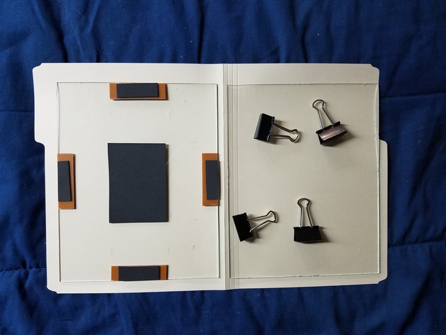
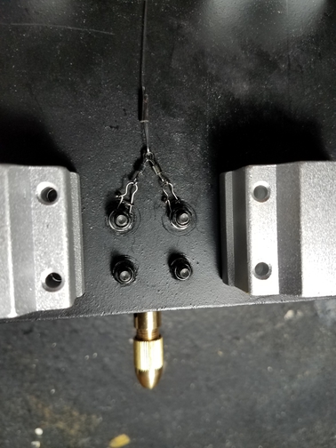
Figure XI. Print Frame Assembly PartsFigure XI is photograph of the print frame before assembly.
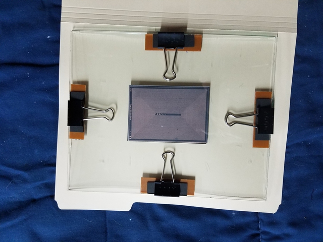
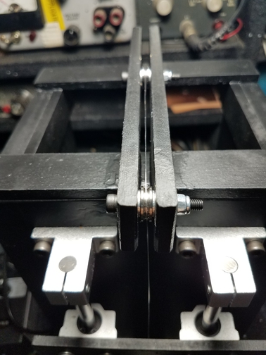
Figure XII. Print Frame AssemblyFigure XII is photograph of the assembled print frame. The PCB is under the artwork. The thickness of shims under the clamps is (nearly,) identical to the thickness under the artwork. Both the top glass plate and bottom glass plate are in a (near,) neutral position and stress. Exposing the PCB, Rationale:There are two programs that will be helpful in designing the PCB UV exposure:
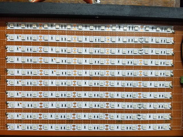
Figure XIII. UV LED ArrayFigure XIII is photograph of the 10 X 15 UV LED array. The array was constructed out of SMD 5050 UV strip LEDs, DC12V 3528/5050 UV Ultraviolet purple waterproof 60led/m Strip lamp black light, and uses the power supply, AC TO DC 12V 5A 60W Regulated Switching Power Supply Adapter for LED Strip Light. These were mounted on 2 Pcs Prototyping Universal Copper Rectangle PCB Print Circuit Board 18cm x 30cm. The UV LED strips are 1/60 of a meter apart, (the same as the UV LED spacing along each strip,) to facilitate hookup of the UV LED strips to terminal blocks which connect to the power supply. The frame was constructed out of scrap lumber. The UV LED array has legs, (of varying length, for experimental purposes,) that are easily detached, (like an in-bed breakfast table.) A setup was made under the SMD 5050 UV LED strip exposure stand of 150 LEDs, 8.25 inches between LEDs and dry film, Ta = 59.3F, (e.g., garage temperature,) from the top, down:
Such that the Rubylith can be slid down, exposing the dry film, more at the top, less at the bottom. The Rubylith was slid down, 1/2" per minute for 20 minutes, to expose the dry etch film at calibrated exposure levels. By eye, there was no change in the blue color after 9 minutes of exposure. Shining a white LED light through the exposed dry film and measuring the light intensity with a LUX meter indicated no difference in the blue color after 11 to 13 minutes of exposure. (Note that this is not a precise measurement-the white LED further exposes the dry film, and the LUX meter sensitivity to UV is down by about 90%.) The SMD 5050 10 X 15 UV LED array exposure time is now calibrated for an 8.5" distance between the LED array and the INSMA 30cm x 5M PCB Photosensitive Dry Film For Circuit Production Photoresist Sheets, at about 9 to 11 minutes. In an effort to reduce the effects of off-contact exposure, the light from the LEDs was narrowed for each LED by reducing the distance between the LEDs and artwork/PCB from 8.5" to 1.0" This reduces the field of light projected on the artwork/PCB for each LED. Using the isotropic.array.py program, and the fact that light intensity decreases with the square of the distance from the source:
Meaning:
For a total exposure time at 1" separation between the UV
LEDs and the dry film of
The emperical data was taken at Ta = 59.3F. To calculate the exposure times for different temperatures, from the Arrhenius Equation: where
Developing the PCB, Rationale:One heaping 1/4 teaspoon of sodium carbonate, 99% Pure SODA ASH (Sodium Carbonate Anhydrous, Washing Soda) (2 lb), is 2 gr. A 50% exposed, double sided, PCB will consume about 1
gallon of dry film developer, 99%
Pure SODA ASH (Sodium Carbonate Anhydrous, Washing Soda) (2
lb), per square foot of PCB, meaning a 10cm X 7cm board
will consume 0.0753 gallon of developer solution, and 1 cup of
developer solution is 0.0625 gallon, or From Dupont
Riston General Processing Guide, (assumed to be
representative of the dry film product INSMA
30cm x 5M PCB Photosensitive Dry Film For Circuit Production
Photoresist Sheets used in this project,) the weight of
the sodium carbonate should be about 1% of the weight of the
water it is dissolved in, i.e., 10 gr. of sodium carbonate per
liter of water. 1 Cup = 240 Milliliter, or the 1.5 cups of
water weighs From Dupont Riston General Processing Guide, (assumed to be representative of the dry film product INSMA 30cm x 5M PCB Photosensitive Dry Film For Circuit Production Photoresist Sheets used in this project):
Note that the time the PCB is in the developer solution in production will be 1.6 to 2.0 times this breakpoint. Three PCBs were scrubbed, (acetone and TSP,) marked with many Expo Vis-A-Vis Wet-Erase Overhead Transparency Markers, Fine Point, Black, lines, and laminated with dry film, twice through the AmazonBasics laminator set on 5 mil, and each developed in a solution made from luke warm water, Ts = ~98F, two heaping 1/4 tsp of 99% Pure SODA ASH (Sodium Carbonate Anhydrous, Washing Soda) (2 lb) per 1.5 cups of water:
Note that there are three methods of developing the PCB. The third is conventional, and has been used successfully by DIY'ers for over 50 years. Only two methods will be pursued in this project, the first and the second methods:
The emperical data for development time methodologies was taken at Ts = 98F. To calculate the exposure times for different temperatures, from the Arrhenius Equation: where Note that there were safety considerations in the design of the development process. Specifically, sodium carbonate is similar to household baking soda. In point of fact, if food grade household baking soda is heated to about 350F in an oven, gas will escape from the baking soda, leaving a white powder-sodium carbonate. Actually, in a pinch, household baking soda can be used instead of sodium carbonate. Rinsing the PCB, Rationale:The rinsing is important, and should be half the developer time, as per Dupont Riston General Processing Guide, (assumed to be representative of the dry film product INSMA 30cm x 5M PCB Photosensitive Dry Film For Circuit Production Photoresist Sheets used in this project.) Etching the PCB, Rationale:From Etching with Air Regenerated Acid Cupric Chloride:
Each 10cm X 7cm PCB is 70 cm^2, or 1.12L if the PCB was double sided, or the one liter polypropylene container, (TashiBox Plastic Food Container / Food Storage / Soup Container with Lids, 32 Ounce - Set of 24,) would contain enough etching solution for two single sided PCBs before regeneration was required. The emperical data for the etching time methodology was taken at Ts = 110F. To calculate the etching time for different temperatures, from the Arrhenius Equation: where Note that there were safety considerations in the design of the etching process. Specifically, the chlorine concentration in the etching solution is about twice that of household bleach, (i.e., "Clorox.") One ALWAYS, (repeat, ALWAYS,) adds acid to water, (HCL to H2O2 in this case, which is the way the solution is made.) An inadvertent spill of the etching solution goes into tap water. It is not as convenient as electrically heated etching solution, but relatively safe. Usually, one liter of the solution is made first, (remember, ALWAYS, HCL into H2O2,) and placed in the container with hot tap water-by the time for the etching solution, it is about 100F. Drilling the PCB, Rationale:For occasional PCB development where precision is not necessary, an Archimedes drill, (for example, In-tool-home Semi-automatic Spiral Drill with Spring Hand Chuck Pin Vise with Twist Drill Bits Set of 21,) is a cost effective alternative for a small number of PCB holes. Although there are commercial drill presses available in the US $50 to $100 range that work well for manually drilled PCBs with holes of 0.9mm = 35 mil, finer line widths usually require a special purpose built drill press.
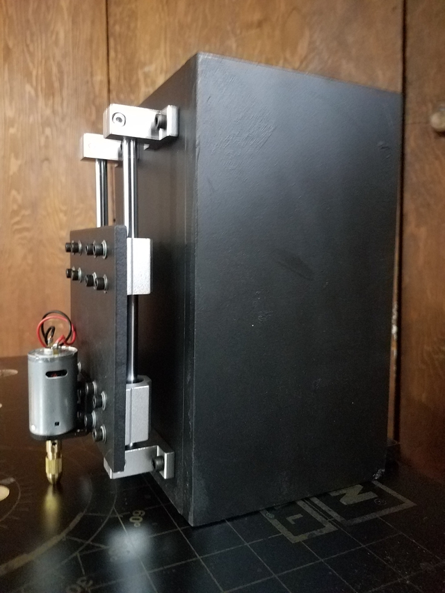
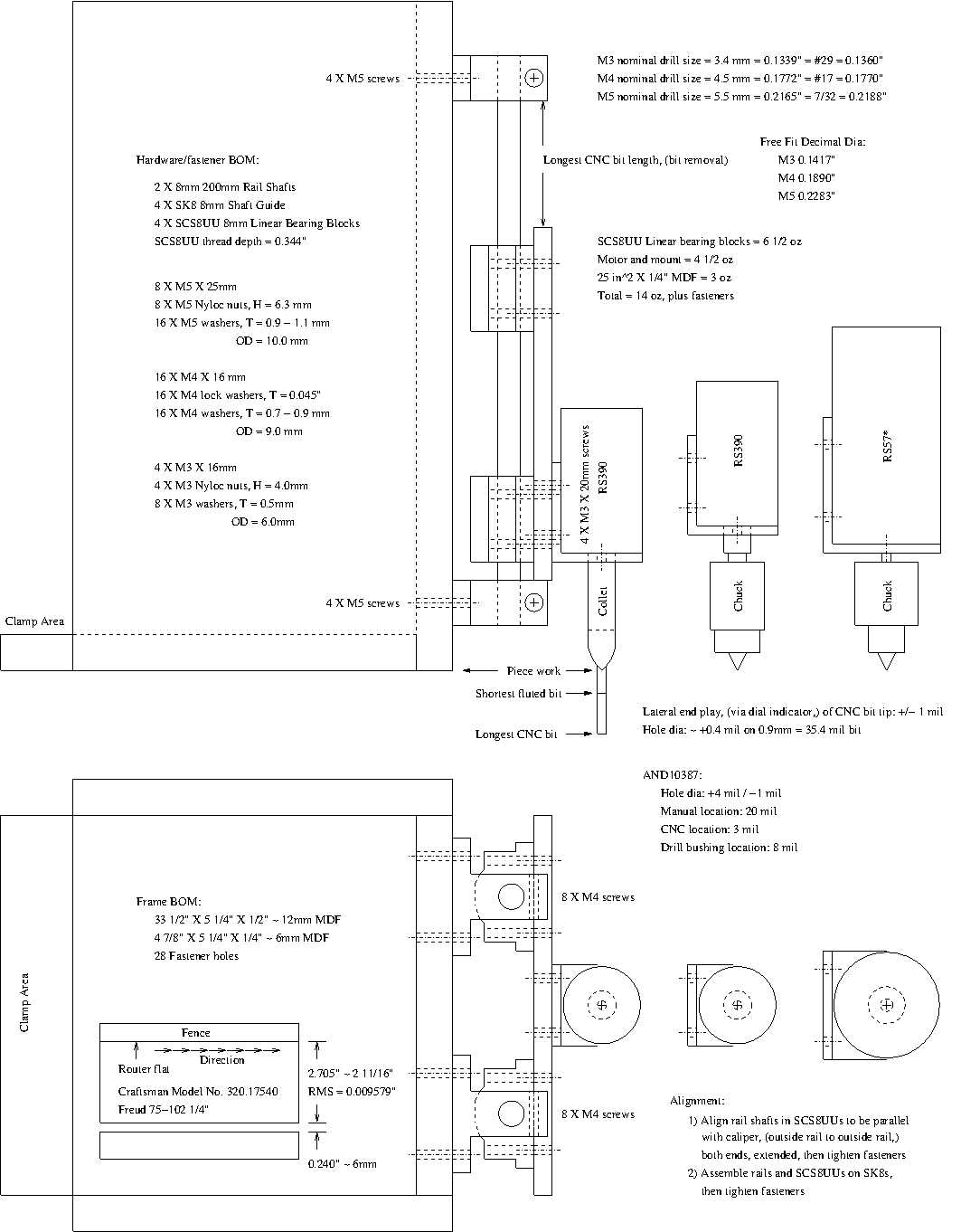
Figure XIV. Drill PressFigure XIV is photograph of a simple, easy to construct, and relatively inexpensive drill press. For precision, it is based on 2Pcs 8mm 200mm Linear Shaft Rod Rail Kit W/ Bearing Block For 3D Printer CNC and Electric Hand Drill DIY set DC12V Motor w/Twist Drill Bits 2.3mm Chuck Bracket which is powered by a AC110V TO DC Adjustable 3-12V 1A Power Supply Adapter for Electric Drill Motor Hand Drill, (not shown,) to control the drill motor speed and 2.3mm+10Pcs 0.5-3.2mm Micro Twist Hand Drill Kit Chuck Electric Drill Bit Collet which has a 1/8" = 3.17mm collet for standard CNC bits with 1/8" shanks. The frame of the drill press was made using a plunge router, an end mill bit, straight edge, 90 degree triangle, electric drill, and a drill guide. All MDF was cut to shape with the plunge router-but simple manual/electric saws can be used, with substantial sanding to true the sides and orthogonality of corners. The cost of the drill press is about US $30, (but shop around at the Internet stores-the prices are very variable, sometimes daily.)
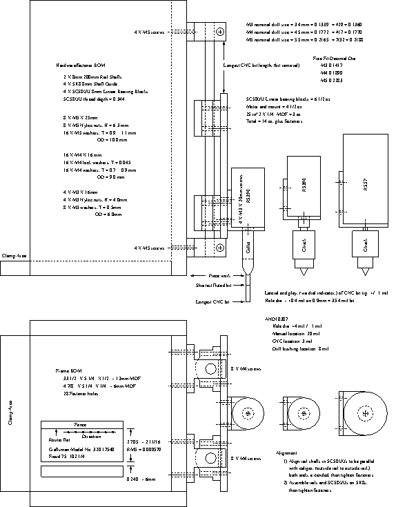
Figure XV. Drill Press Work SheetFigure XV is the drill press work sheet, (large PNG format, or in original XFig format, drillpress28.fig.gz.) The frame is a semi-diagonal tensile field torque box design, (the back and top of the box are not shown in the drawing.) The frame is constructed from 1/2" = 12mm and 1/4" = 6mm MDF. The majority of the pieces are the same width, (and like pieces can be trued by clamping all like pieces together and sanding.) The design is ratiometric and jigging is not required-only clamping during gluing, (preferably with carpenter clamps-duct tape has been used as an alternative.) The objective was a simple structure that could be made with manual tools, (and a lot of sanding,) or, a CNC router table with manual crafted G-code. Chladni Vibrating Plate Resonances: 22,000 rpm is the maximum rating on the motor, or 367 Hz. = rps, a factor of 60, in frequency, below the lowest plate resonance of the drill press. A frequency factor of 60 is -36 dB damping for parasitic vibrations of the motor, (assuming a simple single pole Bode plot response,) adequate for damping motor vibration of the plate. A safety factor of two would seem appropriate, (as always in engineering, and is used throughout this document,) indicating a maximum speed of 10,000 rpm, which corresponds to 5.5V. Note that there is no quill, (the mechanism that moves the drill up and down,) since many have their own opinions on how that should be implemented for PCB work (see Quill Return Alternatives for examples):
Note that there is an alignment procedure in the drill press work sheet. Elaborating:
If standard twist drills are to be accommodated, it may be necessary to increase the length of the rail shafts. The maximum chuck/collet diameter is 1/8", and the 1/8" jobber bit drill length is 2 3/4". Additionally, the drill press can be used for cutting and trimming the edges of PCBs using 10X 1/8" Carbide Flat Nose End Mill CNC Router Bits Double Flute Spiral 17mm USA by locking down the quill, and using a fence guide, (like a table router, or scroll router.) However, the feed rate is quite slow. (The author cuts PCBs with a cheap miter box, and a hack saw with a fine tooth blade.)
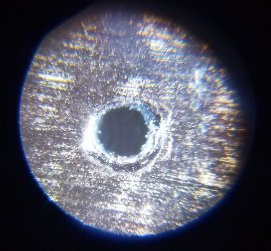
Figure XVI. Photograph of a 0.9mm Hole Made With a 0.9mm CNC BitFigure XVI is a photograph of a 0.9mm = 35 mil hole made with a 0.9mm CNC bit in the drill press. The hole was drilled through from the copper side. The photograph is of the copper side of the hole. The cutting speed was 19,300 RPM, (unloaded,) and the hole was not burnished. To measure the dimensions of the drilled hole, a caliper was set to 35 mils, and photographed:
Figure XVII. Photograph of a Caliper Set to 35 milsFigure XVII is a photograph of a caliper set to 35 mils. Both photographs were printed and held up to light to judge the roundness of the hole in all directions. The two photographs were twisted to measure the diameter of the hole, and found to be 0.4 mil larger than the drill that made the hole. (Note that 0.9mm = 35.433 mils, so the produced hole diameter may be more accurate than the 0.4 mil due to limitations of measurement technique-caliper setting, photographic distortion, etc.) The lateral end play of the 0.9mm = 35 mil CNC drill bit was measured with a dial indicator and found to be +/- 1 mil in all directions. The hole measurements of the drill press are commensurate with AND10387:
For fine line PCB work, note the "Manual location: 20 mil" error in the industry standard specification. To achieve "CNC location: 3 mil" capability, the model airplane servo actuated quill, and 800X 8 LED 2 Mega Pixels USB Digital Microscope Endoscope Camera Video Magnifier to optically align the drill bit over the hole location will be required. This is not necessary for pad diameters of 75 mils and minimum bit diameter of 35 mils.
Figure XVIII. Photograph of a 0.3mm Hole Made With a 0.3mm CNC BitFigure XVIII is a photograph of a 0.3mm = 12 mil hole made with a 0.3mm CNC bit in the drill press. The hole was drilled through from the copper side. The photograph is of the copper side of the hole. The cutting speed was reduced to 15,100 RPM, (unloaded,) and the hole was not burnished. Unfortunately, the author has no provision for measuring the dimensional characteristics. The specific hole was from 10 X 10 array, (100 holes,) which required about 20 seconds a hole, (about 30 minutes, total-most of the time in targeting the drill bit.) Some assistance can be provided by using magnifier glasses, (for example, Beileshi 5Lens Glass Magnifying Visor Magnifier Glasses With 2 LED Professional Jeweler's Loupe Light Bracket and Headband are Interchangeable,) and, perhaps, adding several 100Pcs 5mm White Ultra-Bright LED Light Lamp Emitting Diodes 15000MCD lot DP to the bottom of the adapter plate, aimed at the tip of the CNC drill bit, (perhaps powered by a 5V "wall wort," through a current limiting resistor.) Quill Return Alternatives:There are many quill return alternatives, mostly dependent on user preferences and cost constraints. A few examples are listed below, with the exact parts used for replication purposes-but resourcefulness is appropriate.
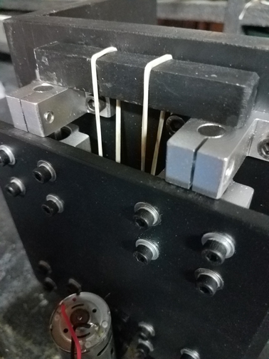
Figure XIX. Photograph of Using Rubber Bands for the Quill ReturnFigure XIX is a photograph of the drill press using simple rubber bands for quill return. The rubber bands will have to be replaced periodically, but for occasional use, it is an effective solution. The rubber bands are available at office supply stores, or the Internet stores. The ones shown are about 2.5" in diameter, and about 1/16" thick.
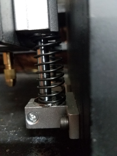
Figure XX. Photograph of Using Springs for the Quill ReturnFigure XX is a photograph of using springs for the quill return. The springs shown are 10 Pcs Small Compression Springs 40mm Long x 10 mm OD (Nominal), which fit quite tightly around the rail shafts. The washers are standard 8mm. The springs are strong, and a lever actuated handle will probably be required, (much like a standard drill press.) Team Associated 1/10 12MM Front Spring Black 3.00 #91326 Sealed have also been used with 10mm washers-but the springs are very strong.
Figure XXI. Photograph of Using a Counter Weight for the Quill ReturnFigure XXI is a photograph of using a counter weight for the quill return. The photograph is the back of the adapter plate where the actuating string for the counter weight is attached. The face plate and motor assembly weigh about one pound. The actuating string will have a tension of about one pound. At least a ten X safety factor was deemed reasonable, and KastKing DuraBlend Monofilament Leader Line, which is at least 20 pound test, was used for the actuating string. The hardware, (all at least 20 pound test,) used was SHELURE Duo-lock Lock Snaps Nice Swivel For Fishing Saltwater Solid Rings Fishing Connector, Dr.Fish Rolling Barrel Fishing Swivel Stainless Steel Black Nickel, and, American Fishing Wire Single Barrel Crimp Sleeves. The counter weight, (of 2 to 3 cubic inches of metal-coins, fishing weights, etc.,) is suspended inside the frame, and attached to the adapter plate in the center, (via the actuating string,) through two CTYRZCH 10pcs 3D Printer Extruder U-groove Guide Wheel Size 4134mm bearings mounted on top of the frame face. This is a nice alternative since the force remains constant to move the drill motor/adapter plate up and down with minimal force. This frees the index finger and thumb of both hands to stabilize the PCB during drilling, the quill being actuated by the smaller fingers on one hand through a small handle rigidly attached to the bottom of the adapter plate.
Figure XXII. Photograph of Using a Counter Weight for the Quill ReturnFigure XXII is a photograph of using a counter weight for the quill return. The photograph is the top of the drill press, and shows the KastKing DuraBlend Monofilament Leader Line running from the adapter plate, over the top of the drill press, and down to a counter weight of about 175 US pennies in a large pill bottle. The CTYRZCH 10pcs 3D Printer Extruder U-groove Guide Wheel Size 4134mm bearings mounted on top of the frame face are visable.
Figure XXIII. Photograph of the via-array test PCBFigure XXIII is a photograph of a test/QA PCB consisting of 988 vias filling a 10 cm X 7 cm PCB, (38 X 26 vias.) The holes were drilled with the drill press and a 0.3 mm ~ 12 mil diameter CNC drill, averaging about 4 seconds per hole, (i.e., a little over an hour for all 988 holes-excluding breaks.) The artwork for the test PCB, via-array.tar.gz, is available as a tape archive. There were no drill bit breakages, (only one bit was used,) and a cursory check of the hole positioning was about 3 mils, RMS, (about 4 mils maximum,) which is commensurate with AND10387:
Installing the collet and CNC bits:Installing the collet is only required for a new motor or new collet.
Run out measurements, (measured before 988 holes, and after, to demonstrate stability):
The latter measurement was made by gently descending the CNC bit onto scrap PCB material copper, and allowing the bit to scratch the copper, (but carefully not making any hole-just scratching the copper surface,) and measuring the diameter of scratched circle with a USB microscope. Of interest is the apparent lack of bit walking.
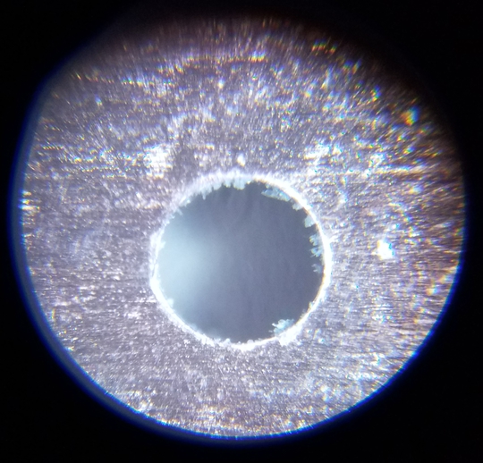
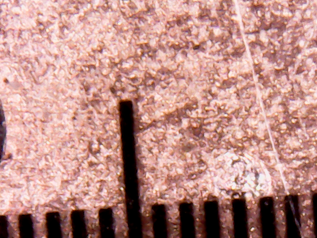
Figure XXIV. Photograph of copper scratch made by the CNC bit tip run outFigure XXIV is a photograph of the copper scratch made by the CNC bit tip run out of the drill press. The calibration ruler small tics are 0.1mm. The diameter of the scratched circle is about 8 mils., smaller than the drill diameters used in DIY PCB development. The CNC bit will self align to the center of this circle to make the hole. Striping the PCB, Rationale:99% Pure SODA ASH (Sodium Carbonate Anhydrous, Washing Soda) (2 lb) is inexpensive since so little is used. A fresh, (as opposed to spent from the developer process,) can be mixed in hot tap water, too. Note that the striping process is nothing more than an intentional over developing of the remaining photo resist on the PCB-which removes the negative photo resist. Soldering the PCB, Rationale:A temperature controlled soldering iron, (for example, Stahl Tools SSVT Variable Temperature Soldering Iron Station,) is highly recommended. Set the minimum temperature that the user is comfortable with. In selection of a soldering iron, verify that replacement tips are available, and preferable that the soldering iron uses "industry standard" tips. Solder should be 63/37 tin/lead, 1.1% flux, 0.031" = 0.8 mm, (for example, Kester Solder 24-6337-8800: #245-No-Clean Flux / Sn63Pb37 / .031 / 1.1% flux,) for PCB through hole components. LicenseA license is hereby granted to reproduce this design for personal, non-commercial use. THIS DESIGN IS PROVIDED "AS IS". THE AUTHOR PROVIDES NO WARRANTIES WHATSOEVER, EXPRESSED OR IMPLIED, INCLUDING WARRANTIES OF MERCHANTABILITY, TITLE, OR FITNESS FOR ANY PARTICULAR PURPOSE. THE AUTHOR DOES NOT WARRANT THAT USE OF THIS DESIGN DOES NOT INFRINGE THE INTELLECTUAL PROPERTY RIGHTS OF ANY THIRD PARTY IN ANY COUNTRY. So there. Copyright © 1992-2017, John Conover, All Rights Reserved. Comments and/or problem reports should be addressed to:
|
Home | John | Connie | Publications | Software | Correspondence | NtropiX | NdustriX | NformatiX | NdeX | Thanks