| john@email.johncon.com |
| http://www.johncon.com/john/ |
|
|
|
||
Direct Coupled Spatial Distortion Reduction Headphone Amplifier |
|||
Home | John | Connie | Publications | Software | Correspondence | NtropiX | NdustriX | NformatiX | NdeX | Thanks
|
The concepts of Spatial Distortion Reduction Headphone Amplifier, and Direct Coupled Stereo Headphone Amplifier, were combined in the tape archive, DCSDRamplifier.tar.gz, which contains the simulations and printed circuit board, (PCB,) development database, (including industry standard Gerber format files, connectivity "rat nests", component vendor and bill of materials, cost estimates, etc.,) for the design of a high quality headphone amplifier, suitable for studio and broadcast applications. The headphone amplifier uses two Lenovo/IBM laptop "bricks" wired in series to produce +/- 20V DC @ 4.5A, (available non-OEM on eBay for under $10 US, each, 50K hours MTBF,) which is reduced to +/- 15 V DC with on-board regulators, (LM7815 and LM7915, which will not be discussed here.) References:
The latter being the most influential, recommending a crossfeed between stereo channels with the following characteristics:
The Headphone Amplifier CrossfeedThe pole is implemented as a low frequency operational amplifier shelf filter circuit. The delay is implemented as an operational amplifier all pass filter.
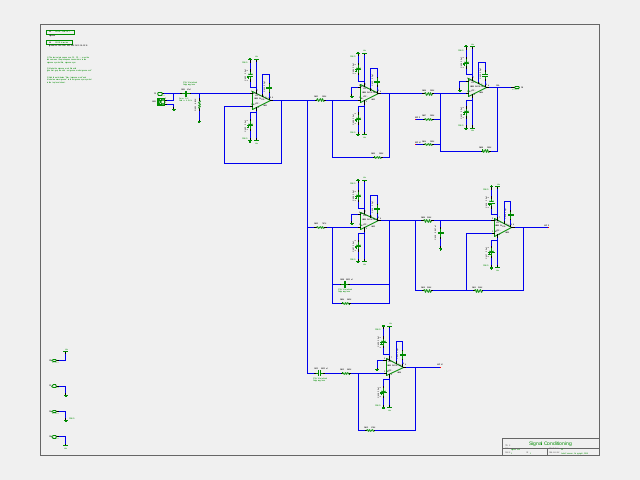
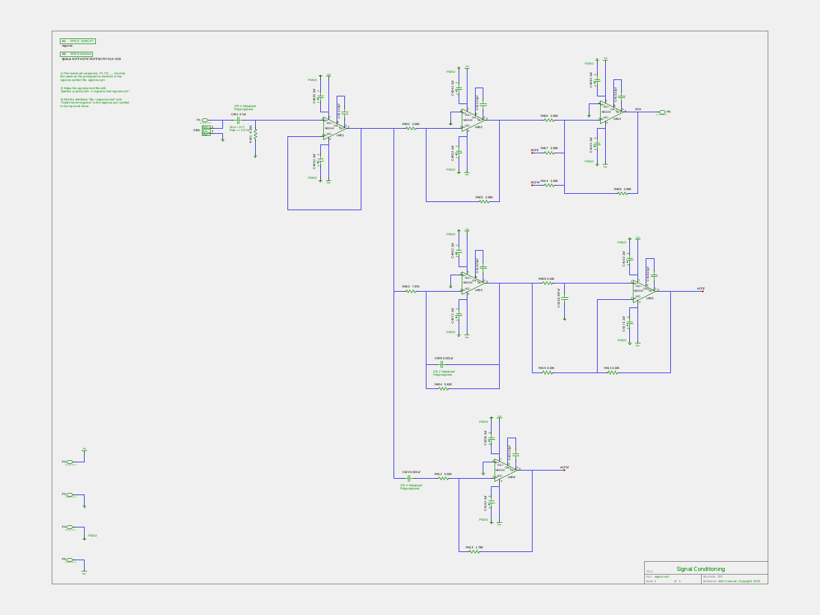
Figure I, (1600X1200,) is the schematic of the signal conditioning circuit for one channel of the the headphone amplifier. (The other channel is identical, except the component reference descriptors are changed to 5XX via a sed(1) script in the ~/Makefile.) The crossfeed from the other channel is BCFlf and BCFhf, (summed in U404, for the low frequency, and, high frequency, respectively,) and, to the other channel, ACFlf and ACFhf, (summed in U504, for the low frequency, and, high frequency, respectively.) The design is a literal translation, (and circuit reductions will be left to the reader,) of the specification, with the following ancillary functions, (which are straight forward, and will not be discussed):
The 300uS delay, (representing the transient time of sound around the human head-from one channel to the other for frequencies < 700 Hz.,) is implemented as an all pass filter, U405. (In Spatial Distortion Reduction Headphone Amplifier, Addendum, it was implemented as a ring buffer in software.) References:
In a linear phase system (with non-inverting gain), both
The Laplace transform of an ideal delay is exponential: (where (where The all pass filter circuit has the following transfer
function, which has the same form as the first order Pade
approximation, with the
The Headphone Power Amplifier
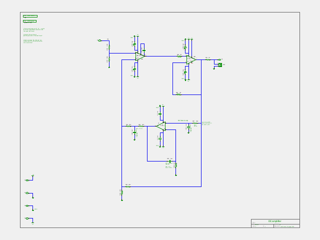
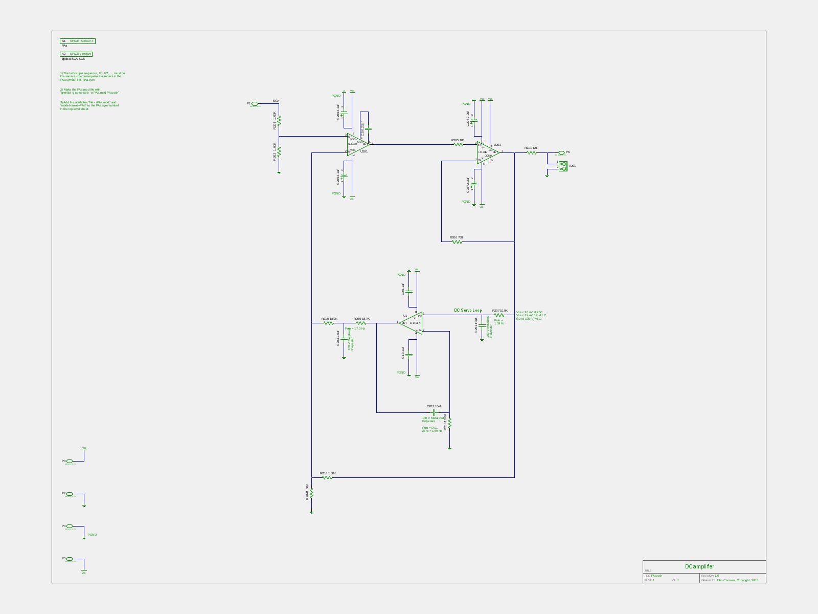
Figure II, (1600X1200,) is the schematic of the DC coupled power amplifier section of one channel of the headphone amplifier. (The other channel is identical, except the component reference designators are changed to 3XX via a sed(1) script in the ~/Makefile.) The headphone amplifier produces a maximum continuous sound level intensity of 100 dB SPL, corresponding to 0 dBFS, consistent with OSHA 1910.95 for sound workers, which is a program level of 85 dB SPL, consistent with IEC 61938, (formerly IEC 268-15,) specifying that headphones will be driven from a 120 Ohm source impedance and a source level of 5 V RMS, maximum, (regardless of headphone impedance.) 5 V RMS probably corresponds to 0 dBFS, which is 100 dB SPL, (or 103 dB SPL, depending on the interpretation of EBU R68-2000 and/or EBU R89-1997.) An input voltage of 0.775 V RMS = 0 dbm should correspond to -15 dBFS = 85 dB SPL, the program level, to within a 6 dB pad for consistency with the other standards, 0 dBm and 0 dBV. There are 5 low frequency poles in the openloop transfer function:
There are 2 low frequency zeros in the openloop transfer function:
See, also: "../dcservo" and "../dcserver/openloop" in the tape archive, DCSDRamplifier.tar.gz, for the closed and openloop gains, respectively, of the DC servo circuit. As a demonstration, altering the value of C203 to 0.1uF, (i.e., decreasing by two orders of magnitude,) results in marginal stability, and further decreasing the value of C203 to 0.01uF results in an unstable, oscillatory, condition. Note that U201, NE5534, is compensated for unity gain stability, (C201,) and has a dominant pole that is substantially higher than other operational amplifiers, (~ 100 Hz.,) with an open loop unity gain frequency of about 8.6 MHz., which is about an order of magnitude less than U202, LT1206, (which is configured for unity gain, and a bandwidth of about 66 MHz., e.g., the high frequency open loop characteristics of the circuit is dominated by the open loop characteristics of U201, NE5534.) U201, NE5534, is stable with C201 = 0pf for closed loop gains greater than 3. The full power bandwidth of U201, NE5534, is about 70 KHz, (adequate for audio,) and the negative unity gain configuration is unconditionally stable. Additionally, the zero, Note that the circuit can correct a maximum Vos, (i.e.,
Note that the input signal low frequency bandwidth must be restricted, (~ 1.0 Hz., minimum, 20 dB / decade, minimum,) to prevent U1, LT1151, from saturating at about +/- 12 V peak output voltage; see: ./sigcona.sch, above. Additionally, the output signal of U1, LT1151, must not
exceed 10 V RMS, ( Power considerations, U202, LT1206:
which is the minimum enclosure size for TA = 70 C, W.C.,
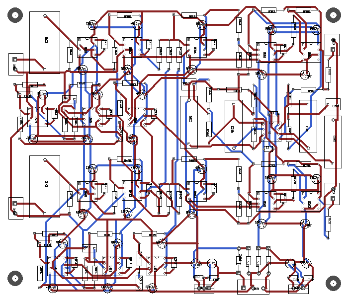
where the enclosure, (at least PC BoardThe PC board is dual layer, (top and bottom, only,) and uses a minimum of 20 mil line widths and 20 mil spacing, (common in linear designs,) which can be manufactured economically at almost any vendor of choice. The boards are designed to be mounted flat, (with 4 fasteners, one in each corner.) The power supplies for the headphone amplifier are two Lenovo/IBM laptop "bricks" wired in series to produce +/- 20V DC @ 4.5A, (available non-OEM on eBay for under $10 US, each, 50K hours MTBF.) The PC board contains +/- 15V regulators, and separate power and signal grounds. The signal path(s) use 275V polypropylene capacitors-a substantial cost reduction can be obtained by relaxing this requirement, (the requirement is the prevailing wisdom in the industry.) The signal path parametrics can be altered, (usually,) with only resistor changes on the PC board-the capacitor values chosen are in the center of the applicable range. The signal conditioning paths use NE5534 Low-Noise High-Speed Audio Operational Amplifiers, (and the designs are compatible with the LT1115 Ultra-Low Noise, Low Distortion, Audio Op Amp, as a direct replacement.) All components are through hole, and SMT components are available. The tape archive, DCSDRamplifier.tar.gz, contains the simulations and printed circuit board, (PCB,) development database, (including industry standard Gerber format files, connectivity "rat nests", component vendor and bill of materials, cost estimates, etc.,) to reproduce, enhance, or modify the circuits used in the headphone amplifier. The design environment used is gEDA. The development system uses gEDA Electronic Design Automation tools, particularly, Gschem(1), for schematic capture and Spice electronic circuit simulation netlist extraction. Ngspice was used for the Spice circuit simulations. RCS was used for version control in the development. The PC board was designed using PC Board Circuit Editor from the gEDA suite.
Figure III is a plot of the stereo headphone signal conditioning and power amplifier printed circuit board, (both channels,) measuring 7.0" X 6.0", and component BOM, DCSDRA.bom. LicenseA license is hereby granted to reproduce this software for personal, non-commercial use. THIS PROGRAM IS PROVIDED "AS IS". THE AUTHOR PROVIDES NO WARRANTIES WHATSOEVER, EXPRESSED OR IMPLIED, INCLUDING WARRANTIES OF MERCHANTABILITY, TITLE, OR FITNESS FOR ANY PARTICULAR PURPOSE. THE AUTHOR DOES NOT WARRANT THAT USE OF THIS PROGRAM DOES NOT INFRINGE THE INTELLECTUAL PROPERTY RIGHTS OF ANY THIRD PARTY IN ANY COUNTRY. So there. Copyright © 1992-2015, John Conover, All Rights Reserved. Comments and/or problem reports should be addressed to:
|
Home | John | Connie | Publications | Software | Correspondence | NtropiX | NdustriX | NformatiX | NdeX | Thanks