| john@email.johncon.com |
| http://www.johncon.com/john/ |
|
|
|
||
Direct Coupled Stereo Headphone Amplifier |
|||
Home | John | Connie | Publications | Software | Correspondence | NtropiX | NdustriX | NformatiX | NdeX | Thanks
|
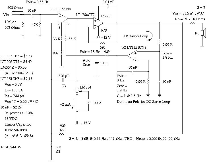
The audio standards for CD and DVD programming have a low frequency cut off specification of 5 Hz., requiring large value output coupling capacitors. This creates a significant issue with the selection of capacitors since they usually have a 2,000 hour lifetime, can not be reverse biased, have non-linear characteristics, and relatively large leakage currents that will put a DC bias on headphones. As a typical example, using Illinois Capacitor part number 227SML016MD8, (220 uF, 16 WVDC, -20%/+20%, 2000 Hrs. MTBF @ 85 C,) the leakage current at 25 C is 35.2 uA at 16 VDC. (It is not clear whether this is a typical, or a maximum, value from the documentation.) As a coupling capacitor, assume 8 V DC, or 17.6 uA leakage current. The leakage current approximately doubles for every 20 degrees C increase in temperature, and increases over the lifetime of the capacitor. Assuming a 16 Ohm headphone, the voltage created by the leakage current would be 16 * 17.6E-6 = 0.282 mV. Assuming a 100 dB/mW power level specification for the headphones, the voltage across the headphone elements would be 0.126 V RMS, and an LSB would be 0.126 / (2^16) = 2 uV-so the leakage current, worst case, would be about two and a half orders of magnitude above an LSB, creating significant DC tension and distortion on the headphone diaphragms. In addition, electrolytic, (and tantalum,) capacitors have non-linearities and hysteresis, (see http://members.aol.com/sbench102/cap.html for particulars,) almost mandating inclusion of the coupling capacitor(s) in the feedback loop for high quality audio reproduction, (not to mention that electrolytic reverse bias considerations would require two capacitors in series, of twice the necessary value, with the junction of the capacitors biased through a resistor to one of the power supply rails to avoid lifetime degradation.) As an alternative, consider a DC servo loop controlling the DC level on the headphones. For example, using the LT1151CN8 chopper stabilized operational amplifier as an integrater, (and dominant pole for the DC servo loop,) the untrimmed worst case offset across the headphone elements would be half of 31.5 uV, or about 8 LSB, worst case maximum, (1 LSB if the full 2 V output of the amplifier were used, and/or could be potentially trimmed to under one LSB.) Figure I, (which is available in larger size jpeg, PDF, or xfig, file formats,) is the schematic of the direct coupled stereo headphone amplifier, with less than 0.001 THD + noise, and a bandwidth that is -3 dB at 0.33 Hz., and 449 kHz.  Figure I. Direct Coupled Stereo Headphone AmplifierThe amplifier has a no-load voltage gain of 4, and is capable of 0.001% THD + noise, 20-20 kHz., and has a bandwidth of -3 dB at 0.33 Hz., and 449 kHz. There is a calc(1) arbitrary precision complex variable calculator script for simulating the amplifier that contains design notes, (most of which appear on this page.) Additionally, there are several, (amplifier performance, open loop gain, DC servo loop performance and frequency response, etc.,) ngspice simulations, using the gschem schematic capture program from the gEDA suite of Electronic Design Automation tools. To use, extract SSheadphoneAmp.tar.gz, and make the various ".mod" files from the LTC.lib spice library, (available from Linear Technology's Design Simulation and Device Models page,) in the various directories. (Note: there is a companion project, Spatial Distortion Reduction Headphone Amplifier, that uses this amplifier.) Small signal analysis:For generality, let the gain of the LT1115CN8 be G1, the gain of the LT1206CT7 be G2, R2 = Zf, R3 = Zi, C3 = Zc, V1 the input signal, V2 the inverting input of LT1115CN8, and V3 and V4 the output of the LT1115CN8 and LT1206CT7, respectively, all of which are complex variables in s = jw. By superposition, V2 in terms of V3:
                     Zi||Zf             Zc||Zi
          V2 = V3 ------------- + V4 -------------
                  (Zi||Zf) + Zc      (Zc||Zi) + Zf
By the definition of gain, G2:
               V4
          V3 = --
               G2
Substituting to eliminate V3:
               V4      Zi||Zf             Zc||Zi
          V2 = -- * ------------- + V4 -------------
               G2   (Zi||Zf) + Zc      (Zc||Zi) + Zf
And rearranging for V4:
                           Zi||Zf            Zc||Zi
          V2 = V4 [-------------------- + -------------]
                   G2 * ((Zi||Zf) + Zc)   (Zc||Zi) + Zf
By the definition of gain, G1 and G2:
                              V4
          V3 = G1 (V1 - V2) = --
                              G2
And, substituting the previous equation into the definition:
                               Zi||Zf            Zc||Zi         V4
          G1 (V1 - V4 [-------------------- + -------------]) = --
                       G2 * ((Zi||Zf) + Zc)   (Zc||Zi) + Zf     G2
Everything is in terms of V1 and V4, rearranging to find the gain of the circuit by isolating terms containing V1 and V4:
                           Zi||Zf            Zc||Zi          V4
          V1 - V4 [-------------------- + -------------] = -------
                   G2 * ((Zi||Zf) + Zc)   (Zc||Zi) + Zf    G1 * G2
Solving for V1:
                 V4               Zi||Zf            Zc||Zi
          V1 = ------ + V4 [------------------ + -------------]
               G1 * G2      G2 ((Zi||Zf) + Zc)   (Zc||Zi) + Zf
And, combining terms:
                       1             Zi||Zf            Zc||Zi
          V1 = V4 [------- + -------------------- + -------------]
                   G1 * G2   G2 * ((Zi||Zf) + Zc)   (Zc||Zi) + Zf
Then, using the definition of the gain of the circuit, G = V4 / V1:
                                  1
          G = ------------------------------------------
                 1              Zi||Zf            Zc||Zi
              ------- + -------------------- + -------------
              G1 * G2   G2 * ((Zi||Zf) + Zc)   (Zc||Zi) + Zf
Note: For idealized amplifiers, G2 = infinity, G1 = 1, and Zc = infinity, the gain, G, would be 1 + (Zf / Zi). Loop gain analysis:Breaking the loop at the input to the LT1115CN8, (with a gain of G1,) with the input grounded, and by superposition, (voltage source ei connected to the positive input of the LT1115CN8,) and voltage source eo connected to the node of Zi, Zf, and Zc, which has voltage V2,) and letting V3 be the output voltage of the LT1115CN8, and V4 be the output voltage of the LT1206CT7:
V3 = ei * G1
and reducing:
          eo = (ei * G1) * ((Zi||Zf) / ((Zi||Zf) + Zc)) +
               (ei * G1) * (G2 * ((Zc||Zi) / ((Zc||Zi) + Zf)))

          eo / ei = G1 * ((Zi||Zf) / ((Zi||Zf) + Zc)) +
                    G1 * (G2 * ((Zc||Zi) / ((Zc||Zi) + Zf)))

          eo / ei = G1 * (((Zi||Zf) / ((Zi||Zf) + Zc)) +
                         (G2 * ((Zc||Zi) / ((Zc||Zi) + Zf))))

          eo            Zi||Zf       G2 * (Zc||Zi)
          -- = G1 * (------------- + -------------)
          ei         (Zi||Zf) + Zc   (Zc||Zi) + Zf
The loop gain equation is quite formidable from an analytical perspective-it has a pole and two complex conjugate zeros, (its a "Miller Effect" mechanism if Zf = 1 / SC3,) in addition to the poles both amplifier's gain equations, (G1 and G2.) Note: If G2 = 1, (a wire,) and Zc = infinity, (C3 = 0):
           eo           Zi
           -- = G1 * (-------)
           ei         Zi + Zf
Amplifier characteristics:
DC servo loop:The DC offset of the amplifier is controlled by integrating the output voltage of the amplifier with half of a LT1151CN8 dual chopper stabilized operational amplifier. The DC error signal feeds back to the input offset adjust of the LT1115CN8, (so it is really an auto-zero technique.) Chopper stabilized op amps do not have sufficient bandwidth for integrating the entire audio range, so there are two filters. The first is a simple RC that reduces the slew rate of the signal fed to the chopper stabilized amplifier, and the chopper positive integrater itself. The positive integrater has a zero at gain = 2, which is canceled by the pole of the simple RC input filter. The unity gain frequency of the DC servo loop is 1 / (2 * pi * RC) = 1.8 Hz. There is an additional 18 Hz. filter in the output of the chopper amplifier to suppress any chopper noise present-this second pole in the DC servo loop is an order of magnitude higher than the unity gain frequency of the DC servo loop, and does not contribute to any instability. The 31.5 uV worst case offset shown on the schematic was obtained by summing the worst case values from the LT1151CN8 data sheet, over the entire temperature, voltage, and make range. An offset adjust could be implemented by a large resistance, spanning the supplies, with a potentiometer near ground that feeds an offset DC bias into the positive input of the LT1151CN8 or into pins 1 or 8 of the LT1115CN8, and adjusting for zero output voltage on the LT1151CN8 with the input to the amplifier grounded, and the DC servo loop disabled. Engineering design:Assuming:
G = 1 + (Zf / Zi) = 1 + (R2 / R3)
The worst case bandwidth of the amplifier is about 2 mHz, maximum, (from the calc(1) script simulations.) The noise voltage would be (1.2E-9 * sqrt (2E6)) * G = (1.2E-9 * sqrt (2E6)) * 4.0 = 6.8 uV, RMS. 2.2 V, (twice Line out = 0 dBu = 0 dBm = 0.775 V RMS; 0dBFS = sqrt (2) * 0.755 = 1.1; unloaded output would be twice this,) output would correspond to 0dbFS = 32767.5, or an LSB would be 67 uV, e.g., the noise floor of the design is about equal to one tenth the quantization noise, or the total noise would not be significantly increased. Input bias current noise for the LT1115CN8 is 2.2 pA / sqrt (Hz). The impedance of the input circuit is less than 600 Ohms, (i.e., the impedance of what is driving the amplifier.) The noise contribution would be 600 * 2.2 pA / sqrt (Hz) = 1.3E-9 V / sqrt (Hz) volts, and is an insignificant noise contribution. For the negative input of the LT1115CN8, the equivalent resistance is 303||909 = 227. The noise contribution would be 227 * 2.2 pA / sqrt (Hz) = 0.71E-9 V / sqrt (Hz), and is an insignificant noise contribution. The 1 / f low frequency noise voltage break point for the LT1115CN8 is about 5 Hz., and is an insignificant noise contribution. The 1 / f low frequency input bias current noise break point for the LT1115CN8 is about 250 Hz, and is about 2.2 pA across sqrt (303^2 + 600^2) = 672 Ohms, (the positive and negative noise voltages add RMS,) or 1.47 nV / sqrt (Hz) at 250 Hz. The integral of 1 / f = ln (f) which is 1.47 nV / sqrt (Hz) at 250 Hz. Therefore, X / 250 = 1.47E-9, or X = 370E-9 V / sqrt (Hz), and 370E-9 * ln (200) - 370E-9 * ln (1.6) = 2.0 uV - 0.17 uV = 1.8 uV, which is an insignificant noise contribution. Overall noise performance, from 5 Hz. to 22 Khz., would be about 6.8 uV of noise, which is about a factor of ten lower than the quantization noise for 16 bit data. The objective of the design was that the amplifier's noise contribution be significantly less than the quantization noise of the input signal. The total system noise-the quantization noise and amplifier noise would add RMS, for an increase in noise of about sqrt (1.1) = 5%, or about a half dB. The overall dynamic range would remain at about 10 log (2^16) = 96 dB, the dynamic range of the input signal. The maximum distortion of the LT1115CN8, (including CMRR,) is 0.002%, or about 1 in 50,000, corresponding to 65535 / 100000 = 1.3 LSB for 16 bit data. Adding the 1 / 0 LSB RMS noise contributed by the amplifier, the amplifier noise plus distortion is about equal to about 1 LSB for 16 bit data. Since the quantization noise and amplifier noise, (including harmonic distortion,) add RMS, the total noise is increased, over the quantization noise, by 41%, or 0.4 LSB for 16 bit data, which is an increase of 3 dB. The maximum slew rate the amplifier must handle is dV / dt = 44000 * 2.2 * PI * 2 = 0.61 V / uS, for a maximum output signal of 2.2 Volts at 44 Khz. The slew rate of the amplifier is limited by the LT1115CN8, which has a minimum slew rate of 10 V / uS, about sixteen times what is required. (Note that if 22000-the sample frequency for 16 bit data-is used as the maximum frequency, the slew rate is 0.30 V / uS, and the LT1115CN8 has a factor of 32 better performance than is required, worst case.) This is an important requirement since slew rate limited intermodulation distortion has odd order products that are the difference of two frequencies, (i.e., a large low frequency signal cross modulating a small high frequency.) Graphing the simulation, the worst case high frequency break point of the amplifier is -3 dB at 10 mHz, (GBW = 10.5E6, 1E6 < GA < 15E6,) giving about 2.5 decades = 50 dB of loop gain at 22 kHz, worst case. Closed loop stability is a formidable proposition from an analytical perspective, since, if Zf = 1 / SC3, it has a pole and two complex conjugate zeros that will split the poles of the amplifier(s) with gain G1 and/or G2. Such an approach would yield very poor parametric sensitivities, (over make tolerances, voltage, temperature, etc.,) However, inspecting the the equations of open loop gain, eo / ei, and the closed loop gain, G, from above:
           eo            Zi||Zf       G2 * (Zc||Zi)
           -- = G1 * (------------- + -------------)
           ei         (Zi||Zf) + Zc   (Zc||Zi) + Zf

                                     1
           G = ----------------------------------------------
                  1            Zi||Zf              Zc||Zi
               ------- + -------------------- + -------------
               G1 * G2   G2 * ((Zi||Zf) + Zc)   (Zc||Zi) + Zf
it can be seen, (if Zf = 1 / SC3,) that at high frequencies, (where 1 / SC3 ~ 0):
           eo        Zi||Zf
           -- = G1 * ------ = G1
           ei        Zi||Zf
and:
                          1                 G2
           G = ------------------------ = ------
                  1         Zi||Zf        1
               ------- + -------------    -- + 1
               G1 * G2   G2 * (Zi||Zf)    G1
Apparently, at high frequencies, (where 1 / SC3 ~ 0,) the feedback loop through Zf is disabled-shorted by C3-and the circuit consists of two unity gain amplifiers in cascade. At low frequencies, (where 1 / SC3 ~ infinity,):
           eo         Zi||Zf   G2 * Zi                      Zi
           -- = G1 * (------ + -------) = G1 * (1 + (G2 * -------)
           ei         Zi||Zf   Zi + Zf                    Zi + Zf
and:
                       1
           G = -----------------
                  1        Zi
               ------- + -------
               G1 * G2   Zi + Zf
meaning that the feedback through Zf = 1 / SC3 is enabled. If Zf = R2, the transition between the two modes of operation occurs at a frequency of S = -1 / R2 * C3). For frequencies less than S = -1 / (R2 * C3), the feedback through Zf is active. For frequencies greater than S = -G / (R2 * C3), the feedback through Zf is inactive, and the only feedback loop is through C3; the amplifier with gain G1 is operating in unity gain, and if it is stable in a unity gain configuration, the design is stable. Note the requirements for unconditional stability:
Note that the requirements for unconditional stability do not depend on parameters other than worst case values from the data sheet and the values of three external components, R2 and C3. The pole, determined by R2 and C3, must be a decade away from 22 kHz, or above 220 kHz. 4.06 times the the pole determined by R2 and C3 must be less than the first pole in the LT1206CT7, which is 10.5 mHz. Therefore:
220 kHz < 1 / (2 * Pi * R2 * C3) < 2.625 mHz
or:
266 pF > C3 > 3.2 nF
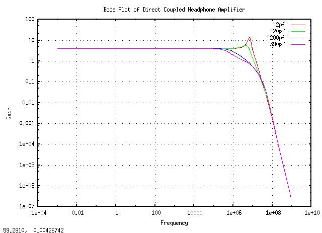
for R1 = 909 and R2 = 303 K. The LM344 provides a current sink on the output of the LT1115CN8 to bias the output stage in Class-A. At high slew rates, the cross over distortion of Class-B output stages adds significant intermodulation distortion to the signal since the slew rate must increase, significantly, to get through zero volts output voltage to steer current through the other complementary output transistors. Figure II is a Bode Plot of the frequency response of the amplifier, made with the calc(1) script, using the worst case, (minimum,) gain bandwidth of both amplifiers, for various compensation capacitor, C3, values. (The plot was made with Gnuplot using the logscale plot command.) With no compensation, (about 2 pF,) the circuit is oscillatory. With 20 pF, peaking is clearly visible, and with 200 pF, the response is almost maximally flat. 390 pF is slightly over compensated. For minimum distortion, 56 pf to 82 pF should be used, (for maximum GBWP, providing maximum gain for audio frequencies,) albeit with potential stability issues-particularly with capacitive loading.
Figure II. Bode Plot Of The Direct Coupled Stereo Headphone AmplifierThermal considerations are quite minimal. The worst case scenario is a +/- 2.2 V P-P = 0 dBFS square wave signal into 2 * 16 = 32 Ohms using a 15 * 1.1 = 16.5 Volt power supply for the LT1206CT7's:
Pd = (16.5 - 1.556) * (1.556 / 32) = 0.726 Watts
The Theta junction-to-air for the TO-220 LT1206CT7 is 50 degrees C / W, or at 27 degrees C, the junction temperature would be 27 + (0.726 * 50) = 63 degrees C at room temperature. If an extended operating temperature range is desired, or the device is going to be tested for extended periods, then a heat sink would be recommended, (for example, mounting the TO-220's on the aluminum chassis for single sided convection cooling; the TO-220's tab is internally connected to the positive voltage, and Theta junction-to-case is 5 degrees C / W; 4 in^2 of sheet aluminum would have a thermal resistance of about 50 / sqrt ((4 * 2.54))^2) = 4.9 C / W.) The point to remember is that for every 10 degrees C increase in junction temperature, the reliability is cut in half, (i.e., whatever is going to fail, will fail twice as fast.) Under normal program content, (producing 85 dB SPL RMS into head/ear phones, which is the maximum permissible,) of -18 dB RMS below 0dBFS, the voltage would be 0.277 V RMS, and the current would be 0.277 / 26 = 10.7 mA, or the power dissipation in each LT1206CT7 would be (16.5 - 0.277) * 0.0107 = 0.174 W, which would be a modest junction temperature rise of 8.7 degrees C. As a simple reliability model, assume electrical/electronic failure is a stochastic, (i.e., a random,) chemical process with a reactrion rate that doubles for every increase in temperature of 10 C, and excluding the power supply, both the LT1206CT7's and LT1115CN8's are the most prone to failure-all are assumed to be rated at 2000 hours = 1 man year of 40 hours per week MTBF at 85 degrees C. (All other components were selected conservatively, and not stressed.) At 27 degrees C, and normal program content, the MTBF would be increased to 2^((85 - 27) / 10) * 2000, which is about 100 thousand hours, or about 50 years, for each of the 2 stressed components at 2000 hours per year usage; the amplifier's overall MTBF would be about 50 / 2 = 25 years of normal operation, (e.g., 40 hours per week, 85 dB SPL program content into head/ear phones, 27 degrees C,) assuming the failure rates to be ergodic. For both amplifiers, it would be about 12.5 years. As an aside, the LT1010CT (TO-220, the tab is ground,) may be a lower cost alternative to the LT1206CT7, at a cost of $3.33. (The 8 pin dip version has a theta J-A of 130 degrees C / W; 0.0677 W normal -18 dB below 0 dBFS at 85 dB SPL would be a junction temperature rise of about 9 degrees C. The LT1010N8 costs $2.92, each.) Also, the LT1097CN8 may be a lower cost alternative to the LT1115CN8, (but may require a 10 K zero adjust); The Vos is 60 uV, Ib = 350 pA, Ios = 350 pA, Vos / T = 1.6 uV / C, Ios / T = 6 pA / C. Additionally, the Japan Radio NJM4580 dual op amp at NJM4580 (available through AmpsLAB,) has attractive noise characteristics, although not as well characterized as the Linear Technology LT1115CN8. The LT6200 has impressive noise characteristics, too-and is characterized at lower supply voltages-as is the LT1206CT7.
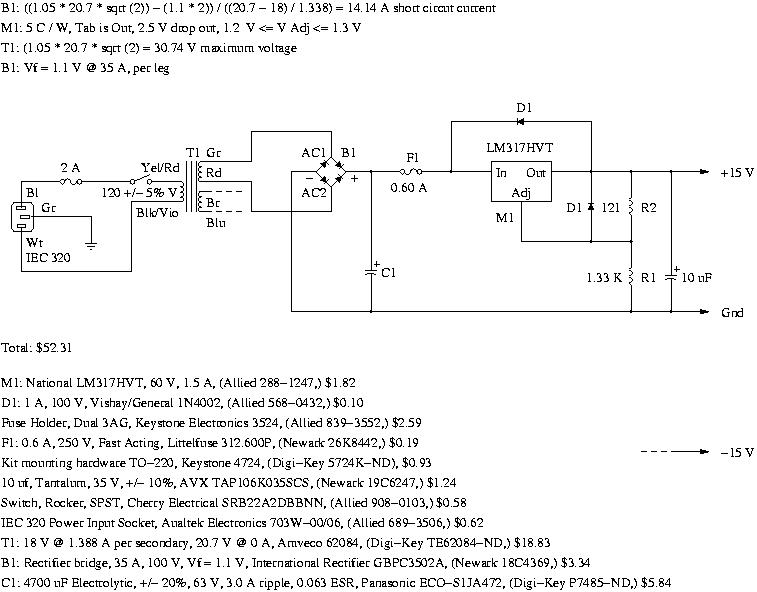
The history of the design:This design is actually quite old; the original design was while I was at Texas Instruments in the early 70's. The design at that time used a Fairchild uA748, (an uncompensated 741,) with feed forward compensation to increase the amplifier's response time, and a TI HIC206 hybrid amplifier as the output current buffer. The TI HIC206 schematic is very similar to the Linear Technology LT1206CT7, and consisted of a pair of matched PNP and NPN discreet transistors, on an alumina substrate-with some thick film resistors-in a TO-99 package. (Later, the basic design was used in high power audio amplifier product lines-for rock concert sound systems-while I was at Motorola, now Freescale, in the late 70's.) Unfortunately, the HIC206 is no longer available, and I needed to upgrade my headphone amplifier to accommodate the high quality, (and inexpensive,) headphones available on the market today-like the Sony EX51LP, which necessitated a re-design with contemporary components. The basic architecture and design is still the same. See, also: National Semiconductor's Application Note AN-1768, "LME49600 Headphone Amplifier Evaluation Board User's Guide," as a modern example. Power supply:15 volt rails are quickly becoming a thing of the past. Unfortunately, the noise performance of the LT1115CN8 is only guaranteed at +/- 18 V. If, as good engineering practice dictates, all power supply components have a safety rating of at least 100%, for voltage breakdown, current, and power dissipation, the number of regulator choices is quite limited. Assuming about 25 V input to the regulators would mean a minimum of 50 V breakdown-and there are only two that are available: the LM317HV, positive regulator, and the, LM337HV negative regulator. Unfortunately, the LM337HV is only available in a TO-3 package, and is relatively expensive, leaving only the LM317HV in a TO-220 package as a viable choice for regulators-despite the fact that its an overkill on current rating for the present application, and the thermal shutdown characteristics can not be used to limit current in the filter capacitor and transformer to half their design limits, (so the supply rails will have to be fused for fault and exception handling.) Figure III, (which is available in larger size jpeg, PDF, or xfig, file formats,) is the schematic of the power supply. 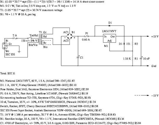 Figure III. Power Supply For The Direct Coupled Stereo Headphone AmplifierThere is a calc(1) arbitrary precision complex variable calculator script for analyzing the currents in the power suppy that contains design notes, (most of which appear on this page.) The capacitor RMS current, transformer secondary RMS current, capacitor peak current, transformer secondary peak current, filter capacitor ripple voltage, (all of which can all be quite large, even under small power supply output currents,) and capcitor RMS voltage have to be computed for a given output current and series pass component values. Note: if all that is necessary is to find the value of a filter capacitor, use:
C = ((i / (2 * pi * f)) * acos (- (vf / vi))) / (vi - vf)
where C is the value of the capacitor, f is the line frequency, vi is the peak voltage on the capacitor, (e.g., the input voltage,) and vf is the minimum voltage on the capacitor, (probably the output voltage of a regulator plus the drop out voltage of the regulator; the capacitor ripple voltage is vi - vf.) What is necessary here is to compute the RMS capacitor current, peak capacitor current, RMS transformer current, peak transformer current, etc., after the capacitor value has been chosen. The voltage input to the diode bridge rectifier, Vpp is the peak-to-peak voltage:
v(t) = Vpp * cos (w * t)
The derivative of the voltage input to the diode bridge rectifier:
dv(t) / dt = - Vpp * w * sin (w * t)
The voltage across the filter capacitor during discharge time:
v(t) = - (Iout * t) / C
The derivative of the voltage across the filter capacitor during discharge time:
dv(t) = - Iout / C
When the derivative of the voltage input to the diode bridge rectifier and derivative of the voltage across the filter capacitor equate, the charge time interval ends, and the discharge time interval begins:
          - Iout / C = - Vpp * w * sin (w * t)
          Iout / C = Vpp * w * sin (w * t)
          Iout / (C * Vpp * w) = sin (w * t)
          sin (w * t) = Iout / (C * Vpp * w)
          w * t = asin (Iout / (C * Vpp * w))
T_begin is when the discharge time interval begins:
T_begin = asin (Iout / (C * Vpp * w)) / w
Vd is the voltage input to the diode bridge rectifier when the discharge time interval begins:
Vd = Vpp * cos (w * T_begin)
Vs is the "effective" starting voltage across the capacitor at t = 0:
Vs = Vd + (T_begin * (Iout / C))
The formula for the discharge time interval is:
v(t) = Vs - ((Iout * t) / C)
Note that a search-for-solution computational method must be used to find the time the capacitor discharge interval ends, i.e., where Vs - ((Iout * t) / C) = - Vpp * cos (w * t), which is part of the calc(1) script. The search is implemented as a recursive binary search on the interval 1 / (4 * f) <= t <= 1 / (2 * f), starting with the variable begin = 1 / (4 * f), and the variable end = 1 / (2 * f); the test for which way to direct the binary search is half way through the interval at t = begin + ((end - begin) / 2), and depending on whether the Vs - ((Iout * t) / C) or - Vpp * cos (w * t) is larger, the end, or begin variable is set to t, the search interval becoming smaller and smaller, at a binary rate, until the end of the discharge time interval is found within a specified error. The charge time interval begins at T_end, and ends at (T_begin + (1 / (2 * f))) for - Vpp * cos (w * t). The peak-to-peak ripple voltage, Vr, is:
Vr = Vpp - (-Vpp * cos (w * T_end))
The capacitor current, Ic(t), during the charge time interval is the derivative of the voltage - Vpp * cos (w * t), multiplied by the capacitor value, C:
Ic(t) = Vpp * C * w * sin (w * t)
Formally, the RMS^2 of Ic(t) in the charge interval will be (1 / t) * integral of (Ic(t))^2 dt, evaluated at T_end and T_begin, where Ic(t) = Vpp * C * w * sin (w * t), which is:
          RMS^2 = ((Vpp * C * w)^2 * ((t / 2) - ((1 / (4 * w)) *
                  sin (2 * w * t)))) / t
evaluated at T_end and T_begin + (1 / (2 * f)). And, the rather formidable formula for the RMS capacitor current during the charge interval, IcRMS:
          IcRMS = sqrt ((((Vpp * C * w)^2 * (((T_begin +
                       (1 / (2 * f))) / 2) -
                       ((1 / (4 * w)) * sin (2 * w * (T_begin +
                       (1 / (2 * f))))))) - ((Vpp * C * w)^2 *
                       ((T_end / 2) -
                       ((1 / (4 * w)) * sin (2 * w * T_end))))) /
                       (T_begin + (1 / (2 * f)) - T_end))
which has an instantaneous peak value, IcP, at the time T_end:
IcP = Vpp * C * w * sin (w * T_end)
RMS^2 of the capacitor current during the discharge interval is 1 / t * integral of - Iout^2dt, evaluated at T_end and T_begin:
(1 / t) * (-Iout^2) t = Iout^2
and the RMS current of the capacitor during the discharge interval is simply, Iout. The total capacitor current, Ic, is:
        Ic = (((T_end - T_begin) / (1 / (2 * f))) * Iout) +
             ((1 - ((T_end - T_begin) / (1 / (2 * f)))) * IcRMS)
The transformer current during the charge interval, IlRMS, is the capacitor current during the charge interval plus Iout:
IlRMS = IcRMS + Iout
The peak transformer current during the charge interval, IlP, is the peak capacitor current during the charge interval plus Iout:
IlP = IcP + Iout
The transformer RMS current, Il, is:
Il = ((1 - ((T_end - T_begin) / (1 / (2 * f))))) * IlRMS
The diode bridge rectifier current is the same as the transformer. The charge time interval begins at T_end, and ends at (T_begin + (1 / (2 * f))) for - Vpp * cos (w * t); the RMS capacitor voltage, VcRMS:
VcRMS^2 = (1 / t) integral v^2(t) dt
For T_begin <= t <= T_end:
          v(t) = Vs - ((Iout * t) / C)

          VcRMS^2 = (1 / (T_end - T_begin)) *
                        integral (Vs - ((Iout * t) / C))^2 dt

          VcRMS^2 = (1 / (T_end - T_begin)) * integral (((Vs^2) -
                        (2 * Vs * ((Iout * t) / C)) +
                        ((((Iout * t) / C))^2))) dt

          VcRMS^2 = (1 / (T_end - T_begin)) *
                        (((Vs^2) * t) - (Vs * ((Iout * (t^2)) / C)) +
                        (((Iout / C)^2) * (1 / 3) * (t^3)))

          VcRMS^2 = (1 / (T_end - T_begin)) *
                        ((((Vs^2) * T_end) - (Vs *
                        ((Iout * (T_end^2)) / C)) + (((Iout / C)^2) *
                        (1 / 3) * (T_end^3))) -
                        (((Vs^2) * T_begin) - (Vs * ((Iout *
                        (T_begin^2)) / C)) + (((Iout / C)^2) * (1 / 3) *
                        (T_begin^3))))
For T_end <= t <= T_begin + (1 / (2 * f)):
          v(t) = -Vpp * cos (w * t)

          VcRMS^2 = (1 / ((T_begin + (1 / (2 * f))) - T_end)) *
                        integral (((-Vpp)^2) * (cos^2(w * t))) dt

          VcRMS^2 = (1 / ((T_begin + (1 / (2 * f))) - T_end)) *
                        (((-Vpp)^2) * ((t / 2) + ((1 / (4 * w)) *
                        sin (2 * w * t))))

          VcRMS^2 = (1 / ((T_begin + (1 / (2 * f))) - T_end)) *
                        ((((-Vpp)^2) * (((T_begin + (1 / (2 * f))) / 2) +
                        ((1 / (4 * w)) * sin (2 * w *
                        (T_begin + (1 / (2 * f))))))) - (((-Vpp)^2) *
                        ((T_end / 2) + ((1 / (4 * w)) * sin (2 * w *
                        T_end)))))
and the rather formidable formula for the total RMS voltage on the capacitor:
          VcRMS = ((T_end - T_begin) / (1 / (2 * f))) *
                      (sqrt ((1 / (T_end - T_begin)) *
                      ((((Vs^2) * T_end) - (Vs *
                      ((Iout * (T_end^2)) / C)) + (((Iout / C)^2) *
                      (1 / 3) * (T_end^3))) -
                      (((Vs^2) * T_begin) - (Vs * ((Iout *
                      (T_begin^2)) / C)) + (((Iout / C)^2) * (1 / 3) *
                      (T_begin^3)))))) +
                      (((T_begin + (1 / (2 * f))) - T_end) /
                      (1 / (2 * f))) *
                      (sqrt ((1 / ((T_begin + (1 / (2 * f))) - T_end)) *
                      ((((-Vpp)^2) * (((T_begin + (1 / (2 * f))) / 2) +
                      ((1 / (4 * w)) * sin (2 * w *
                      (T_begin + (1 / (2 * f))))))) - (((-Vpp)^2) *
                      ((T_end / 2) + ((1 / (4 * w)) * sin (2 * w *
                      T_end)))))))
The line transformer under consideration, (Amveco 62084, Amveco,) is rated at a full load voltage of 18 V RMS, at 1.388 A RMS per secondary, and produces 20.7 V RMS at 0 A RMS, 60 C maximum ambient. The peak voltage would be (1.05 * 20.7) * sqrt (2), (for 120 V RMS +/- 5% line voltage,) or 30.74 V. The maximum current output of the transformer, using the manufacturer's recommended form factor of 1.8, would be 1.388 A RMS / 1.8 = 0.771 A DC. (see the transformer's Technical Notes, for particulars.) The filter capacitor under consideration, 4700 uF Electrolytic, (Panasonic ECO-S1JA472,) is rated at 4700 uF, +/- 20%, 63 V, 3.0 A ripple current, an ESR of 0.063, -4- C to +105 C, and a 3000 Hr. life expectancy. The diode bridge under consideration, (International Rectifier GBPC3502A,) has a 1.1 V forward drop @ 35 A rating per leg, and 0.75 V forward drop @ 1 A and 125 C per leg, and, 0.60 V forward drop @ 1 A @ 25 C per leg. The line frequency is either 50 Hz. or 60 Hz. The output voltage from the diode bridge would be between the ranges:
          ((0.95 * 18) * sqrt (2)) - 2.2 = 21.98 V, Minimum
          ((1.00 * 18) * sqrt (2)) - 2.2 = 23.26 V, Typical
          ((1.05 * 18) * sqrt (2)) - 2.2 = 24.53 V, Maximum
Figure IV, (which is available in larger size jpeg, PDF, or xfig, file formats,) is the power supply's power and voltage absolute maximums. 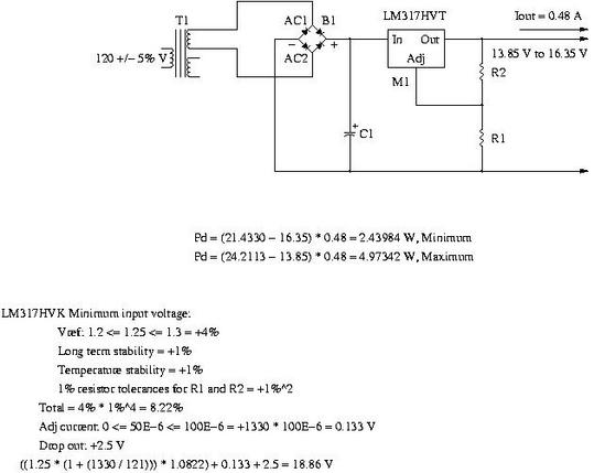 Figure IV. Power Supply Power And Voltage Absolute MaximumsAnd, the output of the calc(1) script:
          Vpp = 21.98, C = 0.00376, Iout = 0.48, f = 50:

          Peak-to-peak capacitor ripple voltage = 1.1413 V,
          Maximum capacitor voltage = 21.98 V,
          Minimum capacitor voltage = 20.8387 V,
          Peak capacitor charging current = 8.2577 A,
          RMS capacitor charging current = 4.6702 A,
          RMS capacitor current = 0.9364 A,
          RMS capacitor voltage = 21.4330 V,
          Peak transformer charging current = 8.7377 A,
          RMS transformer charging current = 5.1502 A,
          RMS transformer current = 0.5609 A
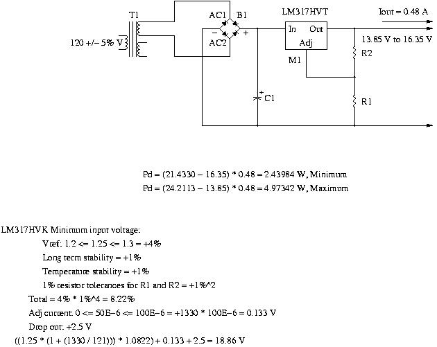
Of interest is the fact that the RMS transformer secondary current and RMS capacitor ripple current are both about a factor of two larger than than the RMS output current, (this is actually a fragment of the output of the calc(1) script-the total output consists of the corner solutions for all worst case parameters. The thermal shutdown characteristics of the LM317HV, (a TO-220 packaged device,) are; a minimum current limit of 1.5 A, typical of 2.2 A, and a maximum of 3.7 A, over 0 C to 125 C, with a maximum junction temperature of 125 C, and Vin - Vout = 5 V. The documentation states that thermal shutdown occurs when the device dissipation is 20 W, or above, (its in the foot note to the device's Absolute Maximum Ratings,) and an output current of 1.5 A. Additionally, there is a current limit graph, (which is assumed to be typical values,) vs the voltage across the device, which for less than 8 volts is 2.2 A @ -55 C, 2.25 A @ 25 C, and, 1.9 A @ 150 C. The short circuit current, (with about 20 V to 22 V across the device,) is about 1.5 A at all temperatures. The junction-to-ambient thermal resistance, Theta j-a, of the LM317HV is 50 C / W, typical, and junction-to-case, Theta j-c, is 5 C / W. The maximum power dissipation at fuse opening is (23.785 - 13.85) * 1.2 = 11.92 W @ Iout = 1.2 A. The junction temperature rise above the case would be 5 * 11.92 = 59.61 C. For the mica insulator with a thermal resistance of 1 C / W, add 11.92 C. For a 3 C thermal resistance heat sink, (3 = 50 / sqrt (A), A = 278 cm^2, or an aluminum sheet, 6.56 inches on an edge, single sided convection, per device,) add 3 * 11.92 = 35.77 C, or a total junction temperature rise of 59.61 + 11.92 + 35.77 = 107.3 C above ambient. If the ambient temperature is 25 C, then the junction temperature would be 132.3 C, at an output current, Iout, of 1.2 A. The efficiency of the power supply is (15 * 1.2) / ((15 * 1.2) + 11.92) = 60.02%. Estimated current consumption:
          Iout = 2 * 81 mA, peak
          LT1206CT7 = 2 * 35 mA
          LT1115CN8 = 2 * 11.5 mA
          LT1151CN8 = 2 * 2.0 mA
          LM317HVT = 1 * (3 mA quiescent +
                          12 mA minimum output current)
          --------------------
          Total = 274 mA,
          (162 mA of DC 0 dbFS signal and, 112 mA quiescent)
A conservative specification would be 0.6 / 1.25 = 0.48 A average continuous output current, with a non-repetitive peak instantaneous current of 0.6 A. The RMS capacitor voltage would be 23.8741 V, for a power dissipation of (23.8741 - 13.85) * 0.48 = 4.81 W. The junction temperature would be 4.81 * 5 = 24.1 C above the case temperature, which is approximately 4.81 C above the mica insulator temperature, for a total of 24.1 + 4.81 C above the chassis temperature. If the chassis is an aluminum sheet, 6.56 inches on an edge, single sided convection, per device, the thermal resistance would be 50 / sqrt (A) = 3 C / W, (A in cm^2); the chassis temperature would be 4.81 * 3 = 14.4 C above ambient. The junction temperature at an ambient temperature of 25 C would be 24.1 + 4.8 + 14.4 = 43.3 C. The maximum operating ambient temperature would be 125 - 14.4 = 110.6 C, (for a junction temperature of 125 C; this exceeds the transformer specification of 60 C ambient, meaning a maximum ambient operating temperature of 60 - 14.4 = 45.6 C = 114.1 F.) 0.48 A would allow an additional (0.48 - 0.271) / 0.0115 = 18 additional LT1115CN8 devices for extensibility. As a simple reliability model, assume electrical/electronic failure is a stochastic, (i.e., a random,) chemical process with a reactrion rate that doubles for every increase in temperature of 10 C. For 25 C ambient, and a junction temperature of 43.3 C, and assuming a 2000 Hr. MTBF at 125 C, the MTBF of each regulator would be about 2000 * (2^((125 - 43) / 10)) = 2000 * 294 = 588,134 Hr., or about 67.1 years of 24/7 operation; about 33.6 years since there are two regulators. For 25 C ambient, and a chassis temperature of 25 + 14.4 C = 39.4 C, and assuming a 2000 Hr. MTBF at 125 C, (Note: Technical Notes states that the transformer is designed for a 65 C rise at full power rating, and a 60 C maximum ambient temperature-from the transformer specification on Miniature Low Profile Transformers-or the maximum internal temperature is 125 C,) at an average secondary current of 0.5609 A RMS, the temperature rise would be 65 * ((0.5609 / (1.388 / 1.8))^2) = 34.4 C, (since the power is proportional to the square of the current,) or the MTBF would be 2000 * (2^((125 - 34.4 - 14.4) / 10)) = 2000 * 196.7 = 393,440 Hrs., which is about 44.9 years of 24/7 operation. (It may be more since the manufacturer's form factor was used as the reference for 2000 Hrs., and not the secondary current.) For 25 C ambient, and a chassis temperature of 25 + 14.4 = 39.4 C, and assuming a 3000 Hr. MTBF at 105 C, the MTBF of each filter capacitor would be about 3000 * (2^((105 - 39.4) / 10)) = 3000 * 94.4 = 383,060 Hrs., or about 32.3 years; 16.2 years since there are two filter capacitors. The total system MTBF, for the LM317HV, the transformer, and the two filter capacitors, would be estimated at about 1 / ((1 / 33.6) + (1 / 44.9) + (1 / 16.2)) = 8.8 years at 25 C ambient, 24/7 usage, and Iout = 0.48 A average continuous current, each regulator mounted on a an aluminum sheet, at least 6.56 inches on an edge, single sided convection, per device. The diode bridge has a reverse bias rating that is at least twice what is applied, and a forward current that is 35 / 0.5609 = 62.4 times what is necessary to source 0.48 A. A remaining issue is fault/exception handling. The LM317HV has a minimum current limit of 1.5 A, a typical of 2.2 A, and a maximum of 3.7 A, which is larger than the transformer and filter capacitor can handle for an indefinite time; an over load or shorted regulator output could damage collateral components. At Iout = 0.48 A, the power dissipation of the devices is 2.49 W to 4.97 W, or a junction temperature rise, with a 3 C / W, 6.54 inch sheet of single sided convection cooled aluminum, of (5 + 1 + 3) * 2.49 = 22.41 C to (5 + 1 + 3) * 4.97 = 44.7 C above ambient-probably well below the 125 C thermal shutdown of the devices. Worst case, for fault/exception fusing with a 0.6 A fast acting fuse, the power supply must be be capable of regulating at 0.48 * 1.25 * 2 = 1.2 A, which is the 200% rating for a 3AG 0.6 A, 250 V fuse, which will open in 5 seconds, maximum at 200% current rating for the fuse. (See Littelfuse, which recommends selecting a fuse rating at 125% of the current rating of the circuit, and specifies a 5 second maximum opening time at 200% of the current rating for the fuse.) Additionally, the fuse has an open time of 4 Hrs., minimum, at 100% of the current rating, 1 Hr., maximum, at 135% of the current rating. Under these conditions, (C = 4700 uF, 0.6 A fuse, Iout = 1.2 A,) the minimum filter capacitor voltage is 19.3172 V, (which is larger than the 18.86 V minimum to the LM317HV,) the RMS capacitor current is 2.3123 A, (which is smaller than the 3.0 A capacitor ripple current maximum for the ECO-S1JA472,) and the RMS transformer current is 1.4118 A, (which is 1.017, or about 2%, larger than the 1.388 A secondary current maximum for the 62084, but is reasonably close to the maximum for a maximum duration of 5 seconds-this is a conservative estimation, see Technical Notes which allows about a 3X current rating for 15 seconds per minute.) The fuses are only rated at 200% current rating for a 5 second open time, maximum, (the maximum at other factors of current rating is unknown,) which means, worst case, that the power supply must operate at the fuse 5 second open current of 2 * 0.6 = 1.2 A, corresponding to an output current of 1.2 A indefinitely. The power dissipation of the LM317HV would be between 1.2 * (19.3172 - 16.35) = 3.56 W and 1.2 * (22.9661 - 13.85) = 10.94 W, corresponding to a junction temperature rise of from 3.56 * (5 + 1 + 3) = 32.0 C to 10.94 * (5 + 1 + 3) = 98.5 C, which would almost be in thermal shutdown for an ambient temperature of 25 C, which is at the maximum of the LM317HV rating. Note that the power supply components are all near maximally stressed for the 5 second open time of the fuse-a reasonable design under fault/exception handling. current value, and have to be replaced.) The alternative is to add collateral circuitry to shutdown the LM317HV regulator under fault/exception situations-which is difficult to do since it does not have control shutdown pins; at least other than grounding the Adj pin, which reduces the regulator output voltage to 1.25 V with a 1.5 A current limit, minimum, (which is an inadequate solution for the collateral components.) The 120 V RMS input could be interrupted via a solid state relay, perhaps by current sensing the transformer current, or disconnecting the output of the regulator via a power FET with low on resistance. Almost any means would require R/S latching during fault/exception handling, and would add circuit complexity, which defeats the advantages of using "jiffy" regulators. Fusing for fault/exceptions seems an adequate and inexpensive alternative. Voltage rating of components; maximum output voltage from transformer = (1.05 * 20.7) * sqrt (2) = 30.74 V:
Or about a factor of 2 = 100% safety margin on component voltages. Current rating of components:
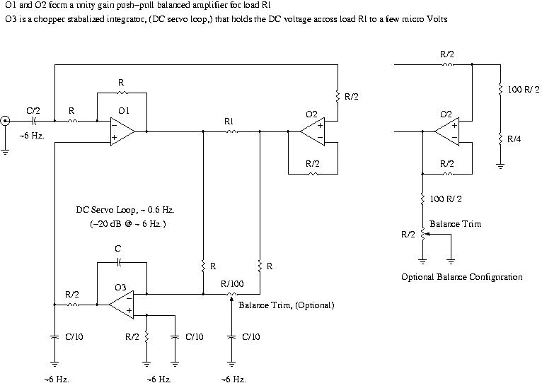
Or about a factor of 2 = 100% safety margin on component currents, fused for 5 second open on manufacturer's minimum operating maximum current, and a factor of 2, (e.g., sqrt (2 * current),) in power dissipation for a maximum of 1 hour. Adaption to high fidelity stereo power amplifiers:Headphone amplifier design is complicated by the fact that each ear piece shares a common ground-it is not possible to use a balanced output amplifier with headphones. Power amplifiers do not have this restriction since high fidelity speakers have two independent terminals-a signal terminal and independent ground terminal. Figure V, (which is available in larger size jpeg, PDF, or xfig, file formats,) is a simplified schematic of a push-pull direct coupled power amplifier. 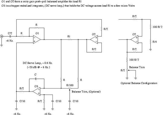 Figure V. Push-Pull Direct Coupled Power AmplifierMusic is recorded and mixed to industry standards. SMPTE RP 155 states that the low frequency cut off of recorded music on a DVD is 5 Hz. The maximum cut off, using Nyquist sampling criteria, is 1/2 of the industry standard 44.1 kHz. sample frequency, or 22.05 kHz. The industry standard for information on a CD is twos complement, 16 bit, binary data, giving a dynamic range, of 2^16 = 65,536 = 96 dB, (the minimum signal level is 1 LSB; the maximum is +/- 32,767 LSBs; 32,767, peak, corresponding to 0 dBFS, and is the maximum signal level that can be produced by a CD; 32,767 peak is a level of 32,767 / sqrt (2) = 23,170 RMS, which corresponds to the maximum power level that can be produced by the data on a CD.) EBU R68-2000 and EBU R89-1997 state that the average programming level on the CD should be -15 dBFS, or a ratio of 5.6, (e.g., -18 dBFS below the peak of 0 dBFS, and the average program level would be 23,170 / 5.6 = 4,137 LSBs.) The minimum level would correspond to a signal amplitude of 1 LSB, which is 72 dB below the average program level, or 85 - 72 = 13 dB SPL, (13 dB SPL is about the same sound level as normal breathing.) The "standard" stereo speaker set up, (used by mixing engineers in the production of a CD,) is to separate the stereo speakers by 12 to 15 feet, (each angled at 60 degrees to face the listener,) and the listener the same distance from each speaker, i.e., the two speakers and the listener form an equilateral triangle, with 60 degree angles. When music for a CD is mixed, it is intended to be played back at a sound pressure level, (SPL,) that is in the lower flat portion Fletcher-Munson Equal Loudness Curves, which is 85 dB SPL for CDs, (92 dB SPL for DVDs,) which also complies with OSHA 1910.95 for 16 hours per day cumulative exposure levels. Note that 85 db SPL would correspond to a CD data level of 4,137 LSBs; the maximum power level would be 100 dB SPL, corresponding to 23,170 LSBs, (and the peak instantaneous SPL-whatever that means-would be 103 dB SPL, corresponding to 32,767 LSBs.) Speaker power output is limited by the physics of sound reproduction, and a sensitivity of 90 dB SPL per Watt at one meter, (with current magnetic technology,) is a good assumption, (cheap PC speakers are usually produce greater than 85 dB SPL per Watt at one meter; expensive commercial units are about 95 dB SPL per Watt at one meter; most high end home units are about 90 dB SPL per Watt at one meter,) and the sound pressure level decreases 6 dB when the distance from the speaker is doubled. As an example of an industry standard reference design, assume the speakers are spaced 13 feet = 4 meters apart, and the listener is 13 feet from each speaker. The sound pressure level at the listener should be 85 dB SPL, half supplied by each speaker, or each speaker should produce 85 - 6 = 79 dB SPL. At two meters, (half the distance to the speaker from the listener,) the SPL would be 85 dB SPL. At one meter from the speaker the sound pressure would be 91 dB SPL, or each speaker would require about one Watt to produce a standard CD programming level of 85 dB SPL at the listener's position. Assuming an 8 Ohm speaker, the average program voltage at the speaker terminals would be sqrt (8) = 2.8 Volts RMS. The maximum level on the CD would be 15 dB-a ratio of 5.6-above the average program level which corresponds to 2.8 * 5.6 = 15.9 Volts RMS, (i.e., 32 Watts per channel.) The instantaneous peak would be sqrt (2) * 15.9 = 22.5 Volts. In Figure V, the supply rails would be +/- 11.25 Volts, or about +/- 12 Volts. Note that the center of the load resistance, Rl, is a virtual ground; each amplifier driving a 4 Ohm load, meaning the peak current would be 12 / 4 = 3 Amperes for each channel of the stereo amplifier. Note that the requirements for the reference design can be met with the LM3886 which is available through the electronic suppliers on the Internet, (Allied Electronics, etc.,) for $5-$10 US in small quantities. The power supply rejection ratio is quite high, and a regulated power supply may not be necessary, (a substantial cost savings in heat sinks, alone,) and the quiescent current control in the output stage, since its a monolithic IC, is superior to discreet implementations. The thermal management, current limiting, etc., since its an IC, are quite adequate, too-and superior to discreet designs. Additionally, there is a package version with an isolated tab, (which facilitates home construction, since the heat sink would not have to be connected to the negative rail-creating an electrical hazard which is usually solved by putting the heat sink inside the case, which is counter productive for thermal management.) If cost is an important design criteria, the chopper stabilized operational amplifier could be replaced with a low offset, (50 micro Volts, or less,) amplifier-and the balance trim may not be necessary in production units. Note that the amplifier BOM cost is about the same as a capacitive coupled design that would drive 8 Ohms at 5 Hz., (requiring about 4,000 uF coupling capacitor,) and has none of the reliability issues. Additionally, circuitry would have to be added to Figure V that nulls equal, but opposite, DC potentials across the load, Rl. As a closing note, Western music is based on even order harmonics, and Western ears are very sensitive to odd order distortion products. Balanced push-pull amplifiers tend to cancel third order products, (this is probably one reason many musicians claim vacuum tube amplifiers produce superior sound quality when compared to semiconductor amplifiers; vacuum tube power amplifiers are inherently balanced push-pull output transformer designs.) The cross-modulation and inter-modulation characteristics of the reference design should be quite good. A note about power dissipation architecture in class B amplifiers. Consider a class B amplifier with an output voltage, Vo, into a load resistance, Rl, driven by power supply rails, +/- Vcc. Then, the output current, Io:
Io = Vo / Rl, Vo < Vcc
The input power, Pi:
Pi = Vcc * Vo / Rl
And, the output power, Po:
Po = Vo^2 / Rl
The amplifier dissipation, Pd:
            Pd = Pi - Po
            Pd = (Vcc * Vo / Rl) - (Vo^2 / Rl)
Which is a parabolic equation, with a local maxima. Taking the derivative of the amplifier dissipation, Pd, with respect to the output voltage, Vo:
d Pd / d Vo = (Vcc / Rl) - (2 Vo / Rl)
and equating to zero for the maxima:
Vo = Vcc / 2
which is 1/4 of the maximum power output, or -12 dB SPL, which is very close to the -15 dBFS standard program level for a CD recording, (a peak of output voltage of Vcc being 0 dBFS). Note that the maxima does not occur at maximum power output of the amplifier, (it occurs at 1/4 power output.) Note that:
Po = Vcc^2 / (4 Rl)
And:
Pi = Vcc^2 / (2 Rl)
for an efficiency, Po / Pi, of 50% at the maxima of the amplifier power dissipation, (which happens, also, to be near the program level of a CD recording, at a volume level that the amplifier is capable of reliably producing, including instantaneous peak output voltage amplitude.) So, to calculate the power dissipation, Pd, requirements of the finals in a class B amplifier, divide the maximum power output of the amplifier by 4, (i.e., divide by 8 for the dissipation requirements of each push-pull class B final.) LicenseA license is hereby granted to reproduce this design for personal, non-commercial use. THIS DESIGN IS PROVIDED "AS IS". THE AUTHOR PROVIDES NO WARRANTIES WHATSOEVER, EXPRESSED OR IMPLIED, INCLUDING WARRANTIES OF MERCHANTABILITY, TITLE, OR FITNESS FOR ANY PARTICULAR PURPOSE. THE AUTHOR DOES NOT WARRANT THAT USE OF THIS DESIGN DOES NOT INFRINGE THE INTELLECTUAL PROPERTY RIGHTS OF ANY THIRD PARTY IN ANY COUNTRY. So there. Copyright © 1992-2012, John Conover, All Rights Reserved. Comments and/or problem reports should be addressed to:
|
Home | John | Connie | Publications | Software | Correspondence | NtropiX | NdustriX | NformatiX | NdeX | Thanks