| john@email.johncon.com |
| http://www.johncon.com/john/ |
|
|
|
||
Distortion Considerations in Audio Power Amplifier Circuit Topology |
|||
Home | John | Connie | Publications | Software | Correspondence | NtropiX | NdustriX | NformatiX | NdeX | Thanks
The (Very,) Basics of Human HearingHuman hearing does not have a flat frequency response, and the frequency response is sensitive to Sound Pressure Level, (SPL,) as demonstrated in the Fletcher Munson/ISO 226:2003, equal loudness curves. The ImplicationMusic is recorded for playback at about 85 dB SPL, (100 dB SPL on music peaks,) where the equal loudness curves are almost flat. Any other SPL setting will result in music that is out of balance, i.e., apparently too much bass and treble, (or too little,) relative to the the program level. See: EBU R68-2000 and EBU R89-1997 for technical particulars. A program level of 85 dB SPL is, also, consistent with OSHA 1910.95. See, also: The Artificial Ear Dilemma: The challenges of modern handset testing, Gunnar Rasmussen, for the implications of equal loudness curves when using headphones. Importantly, note that there is a minimum threshold of human hearing, (MTH,) and SPLs that are less than the MTH can not be heard by humans, and the frequency response of the MTH is not flat, and varies with frequency. It is the MTH that is important to the "hearable" distortion in sound systems.
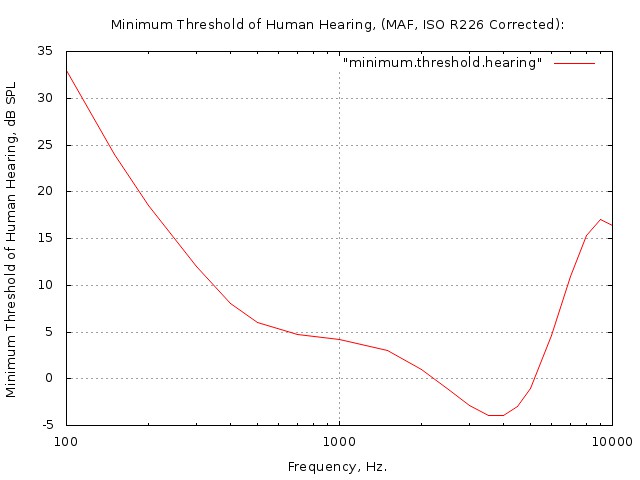
Figure I is a plot of the Minimum Threshold of Human Hearing, (MAF, ISO R226 Corrected.) MAF is Minimum Audible Field, the threshold sound pressure at the listener's position, [listener absent] due to a sound source in front of that position. SPLs lower than the graph can not be heard by humans, and, SPLs higher than the graph can.
Note the implications:
Before proceeding further, one other item has to be
addressed, and that is the listening environment. It is a
popular misconception that ambient room noise will be larger
than the distortion products of almost any sound
system. Although the total ambient noise SPL in a room can be
significant, the Acoustic
Mass Law filters the ambient noise as a single pole
filter, (i.e.,
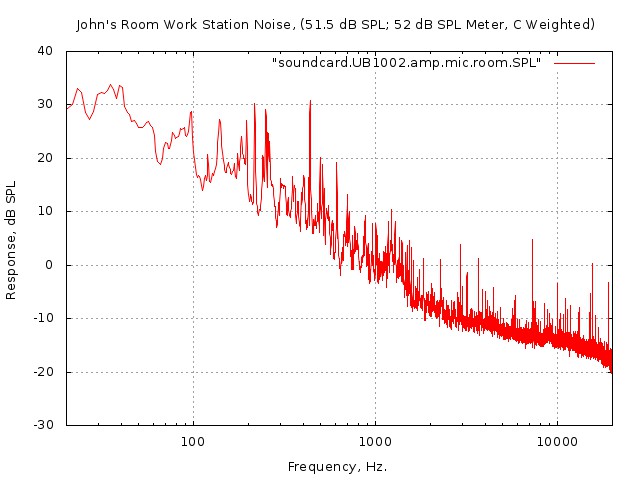
Figure II is a plot of the frequency spectrum of noise in a
typical home small office. The data was taken with a
microphone from the Using the
Panasonic WM61A as a Measurement Microphone page, and baudline(1) was used for
the spectrum analysis. Although the room has a moderate amount
of noise, (about 52 dB SPL, as confirmed with a calibrated
sound level meter,) the Any distortion products in the 2KHz. to 5KHz. frequency range that are above -5 dB SPL can be heard by humans, (although 0 dB SPL, is often used in the industry.) A fair question is "where do the distortion products come from?" and the answer is non-linearities in the sound system components, (microphone, amplifiers, speakers, headphones, etc.) For example, consider a pure sine wave being processed by a sound system component with a square law characteristic, (like a vacuum tube, or field effect transistor, FET.) From the trigonometric identity: Noting that a sine wave, of 2KHz. input to the square law device would produce a distortion product at 4KHz., where the minimum level of human hearing is most sensitive. Now, for example, consider the same sine wave being processed by a sound system component with an exponential law characteristic, (like a bipolar transistor.) From the trigonometric identity, (for the third order in the exponential): These are simple examples of the distortion products in sound system components, and how they are generated, (i.e., Intermodulation products.) However, it is far more complicated when at least two sine waves with different frequencies are being handled by the components, particularly in devices with exponential law characteristics: The result is various combinations of sound system distortions with frequencies of the form: For example The ImplicationsAs a worst case, (WC,) design scenario, any sound system component should be able to handle peaks of 100 dB SPL, while producing a program level of 85 dB SPL, and any spurious distortion products should be below the minimum threshold of human hearing, (MTH.) The most difficult part of the audio spectrum to achieve this design scenario is those distortion products that are in the frequency range of 2KHz. to 5KHz. In this frequency range, the distortion products should be less than -5 dB SPL, (0 dB SPL is acceptable,) which means the distortion products should be less than -105 dB SPL below the maximum of 100 dB SPL. This is not trivial to achieve, since the only viable solution is Negative Feedback. Consider a unity gain amplifier, with
The DesignsThe remainder of this page will explore circuit topologies for low distortion audio power amplifiers. The tools used are available at one's favorite Linux repository, (at no cost.) gEDA Electronic Design Automation tools, particularly, Gschem(1), was used for schematic capture and Spice electronic circuit simulation netlist extraction. Ngspice was used for the Spice circuit simulations The design work sheets and data bases for the amplifier development are available in a single tape archive format, (TAR file, using RCS for version control,) from power-amp-distortion.tar.gz, (and is almost 40 MB in size,) which will install the following directories:
The designs are all ratio metric in the sense that the quiescent currents in an entire circuit depends only on resistors, (one or two,) spanning the supply voltages, Vcc and Vss, to accommodate system application, integration and ancillary requirements. All of the designs will be walked through in the above corresponding order, and comments made. The analysis was extensive, (particularly where distortion products were concerned,) but will require installation of the software tools for complete documentation of the results. A word of caution to the uninitiated, these amplifiers have gain bandwidth products that extend into the VHF range, (several hundred MHz.,) and one must be familiar with high frequency layout techniques, frequency compensation and feedback fundamentals of control systems-not to mention access to some expensive test and development equipment, (a several hundred MHz. oscilloscope as a minimum.) Additionally, competency with Spice frequency, distortion and transient analysis, (both closed and breaking closed loops to obtain open loop characteristics of frequency and distortion,) will be required for a complete evaluation, of the power-amp-distortion.tar.gz tape archive.
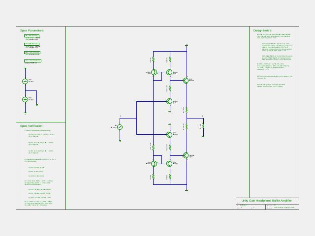
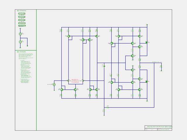
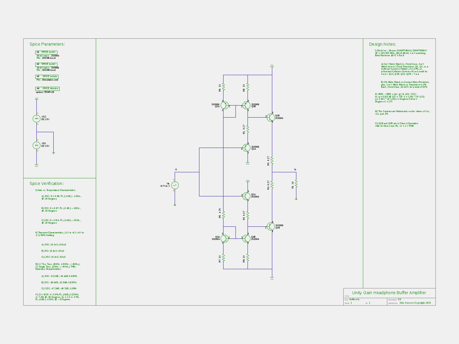
Figure III, (1600X1200),(3200X2400), is the schematic of the headphone buffer amplifier in the headphone-buffer-amp/ directory. The sub-directories, (Zi/, Zo/, distortion/, distortion/two-tone, simple/, simple/distortion, transient/,) contain the analysis. The 25C second order distortion at 2KHz. is 0.078% = -62.2 dB, and the two tone distortion, (6KHz., and 8KHz.) at 4KHz. is 0.33% = -49.5 dB, (both relative to maximum output = 0.7 V RMS into 16 Ohms.) The gain varies from 0.8 to 0.9 over military temperature range, and the frequency response is over 100MHz. to accommodate inclusion in the closed loop of a high quality audio operational amplifier front end, (as used in the Direct Coupled Stereo Headphone Amplifier project without adding another pole in the frequency transfer function,) and reduce the distortion levels to acceptable levels of the design requirements. The output drivers are in class A operation, (in the sense that neither output driver transistor turn completely off,) with an output of 0.7 V RMS into 16 Ohms. The total cost of the semiconductors in the circuit is under US $2, but all the transistors are matched pairs, (meaning available packages are SOT, only.)
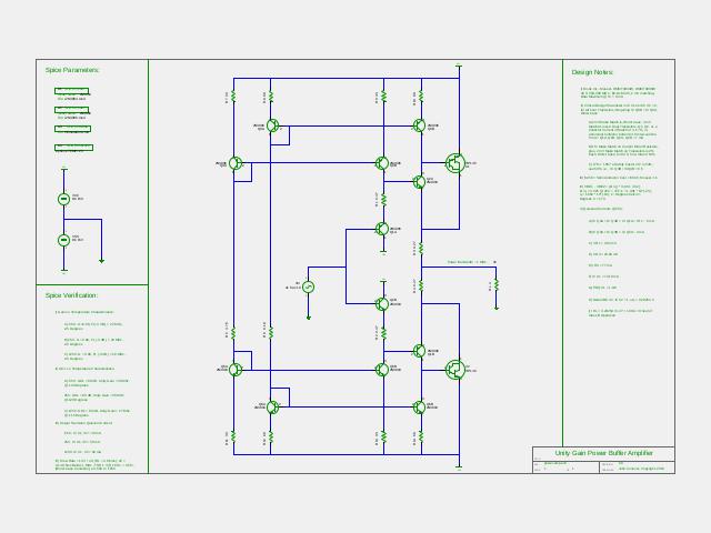
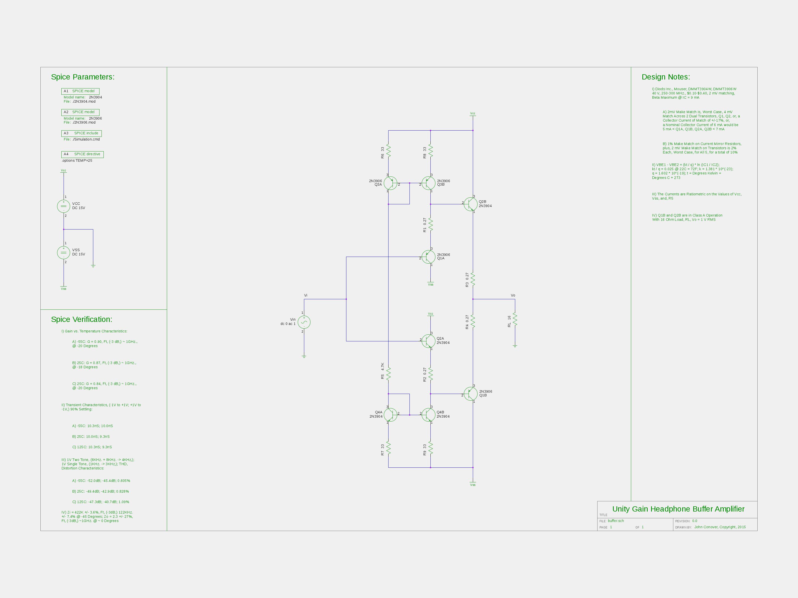
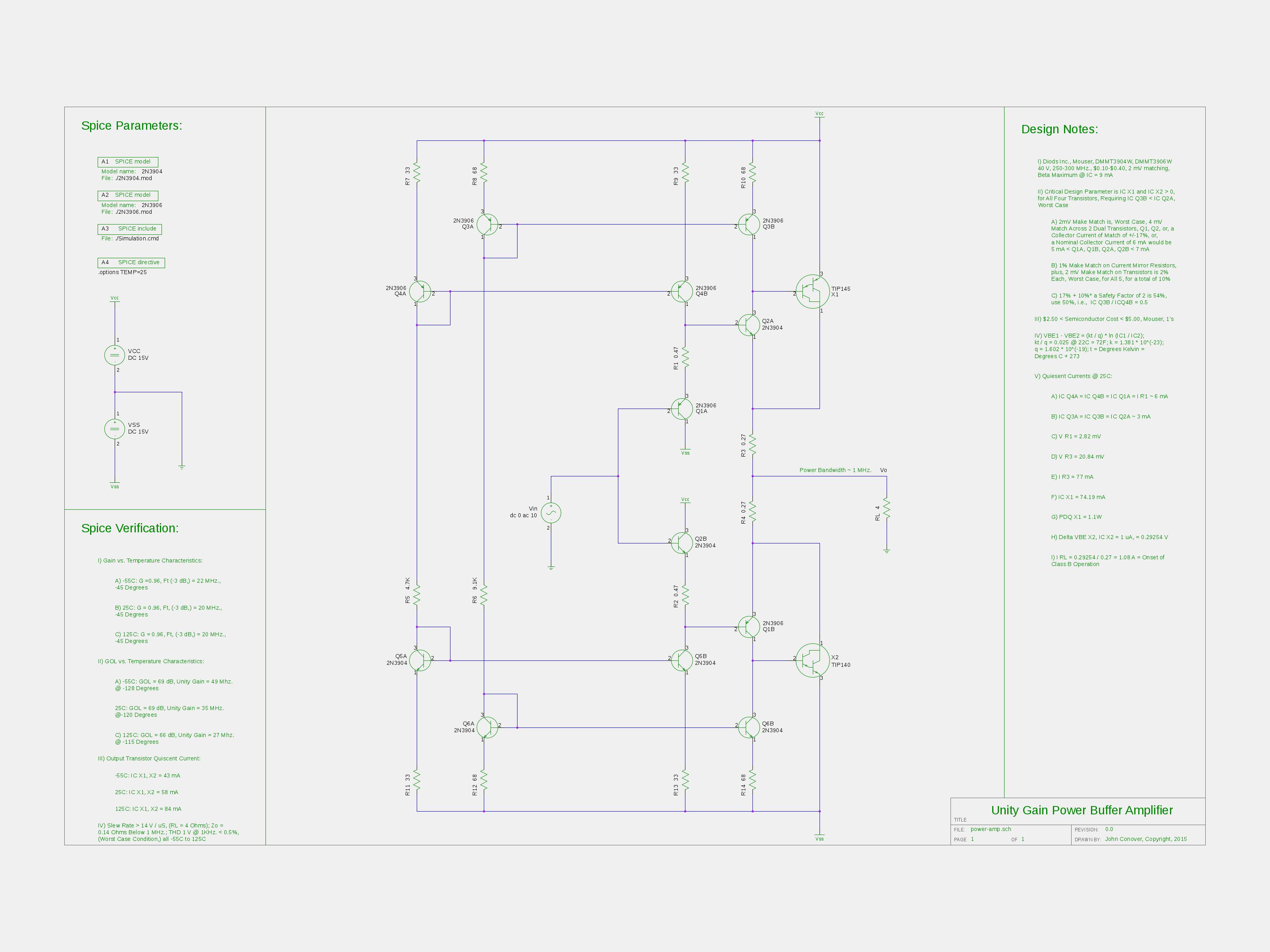
Figure IV, (1600X1200),(3200X2400), is the schematic of the preceding design, with complementary Darlington transistors added, in the power-amp/ directory. The sub-directories, (DC/, Zi/, Zo/, distortion/, distortion/two-tone, noload/, openloop/, openloop/distortion/, openloop/distortion/two-tone, transient/, transimpedance/,) contain the analysis. The 25C second order distortion at 2KHz. is 0.0015% = -96.5 dB, and the two tone distortion, (6KHz., and 8KHz.) at 4KHz. is 0.031% = -70.2 dB, (both relative to maximum output = 7 V RMS into 4 Ohms.) The gain varies from 0.9 to 1.0 over military temperature range, and the -3 dB frequency response is over 20MHz., (unity gain is almost 100 MHz.,) to accommodate inclusion in the closed loop of a high quality audio operational amplifier front end, (as used in the Direct Coupled Stereo Headphone Amplifier project with appropriate frequency compensation,) and reduce the distortion levels to acceptable levels of the design requirements. The total cost of the semiconductors in the circuit is under US $6, but all the transistors, (excepting the Darlington output drivers,) are matched pairs, (meaning available packages are SOT, only.)
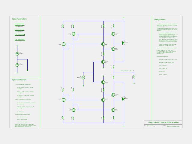
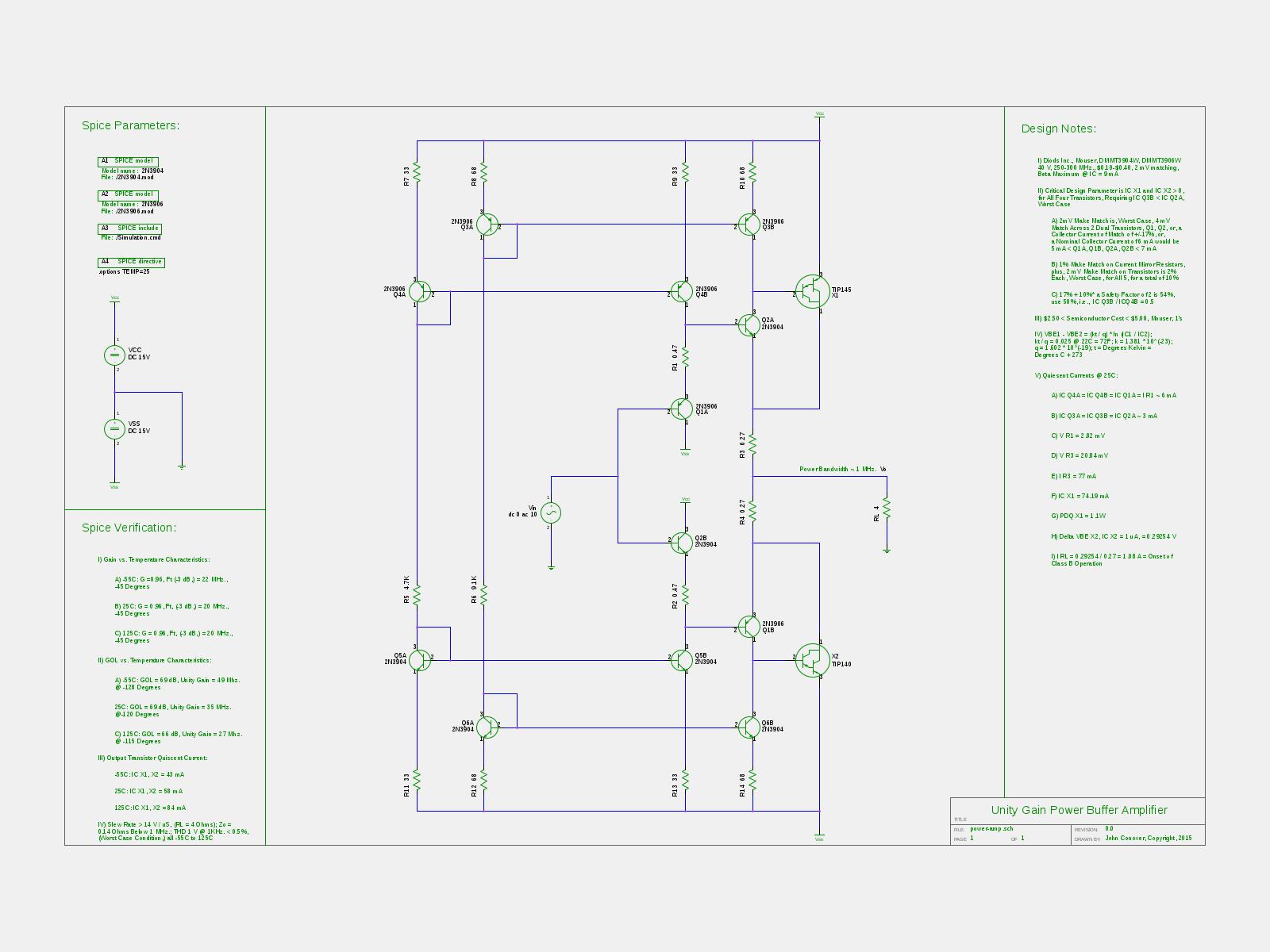
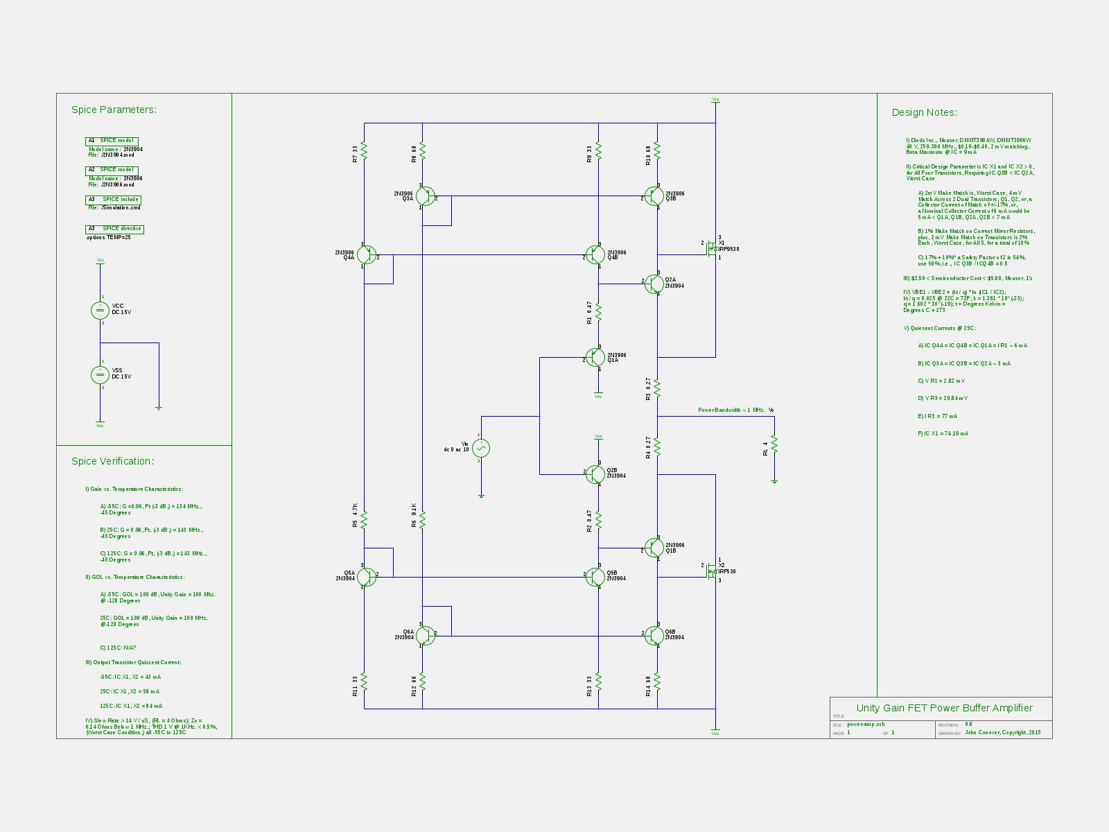
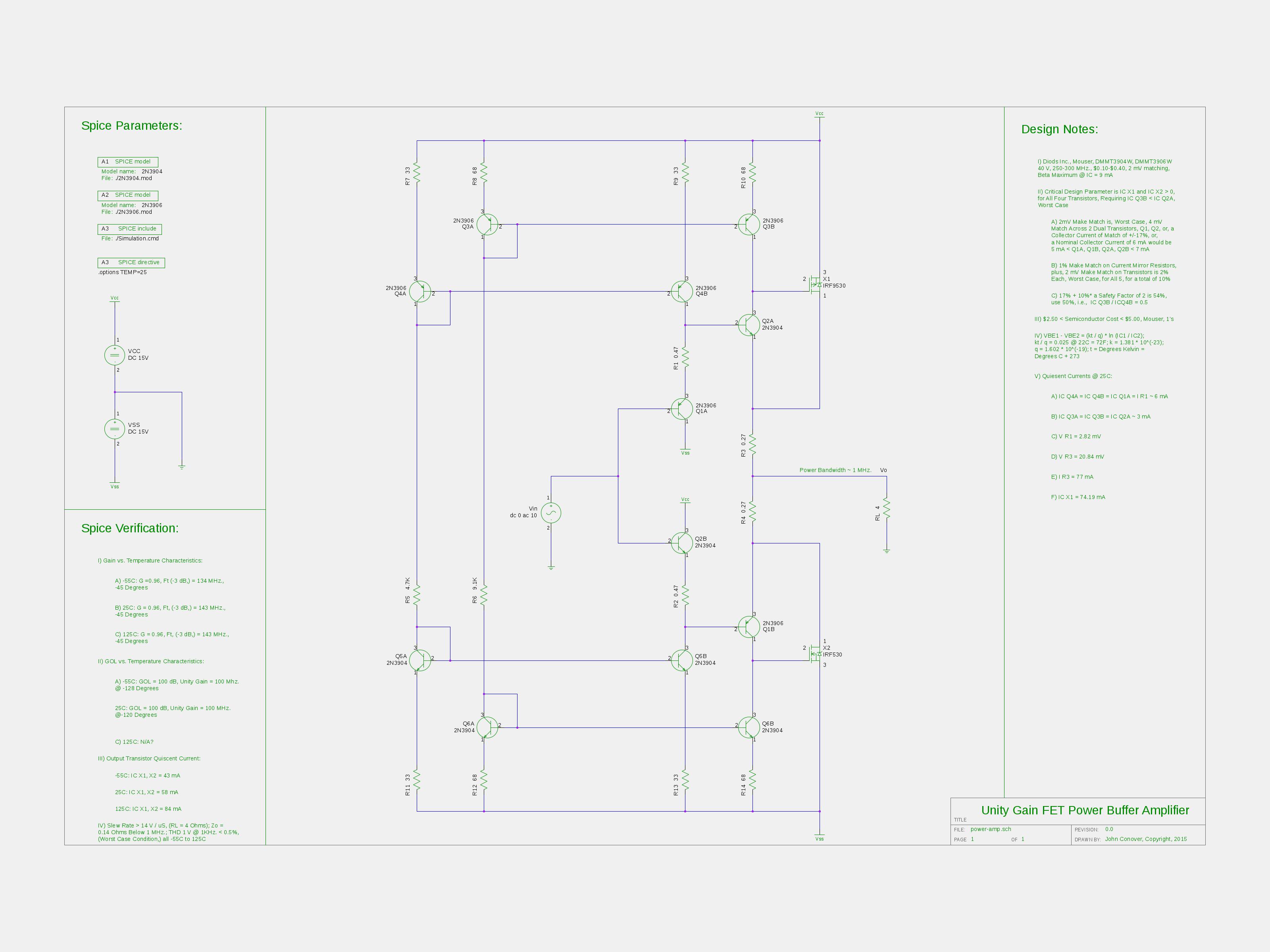
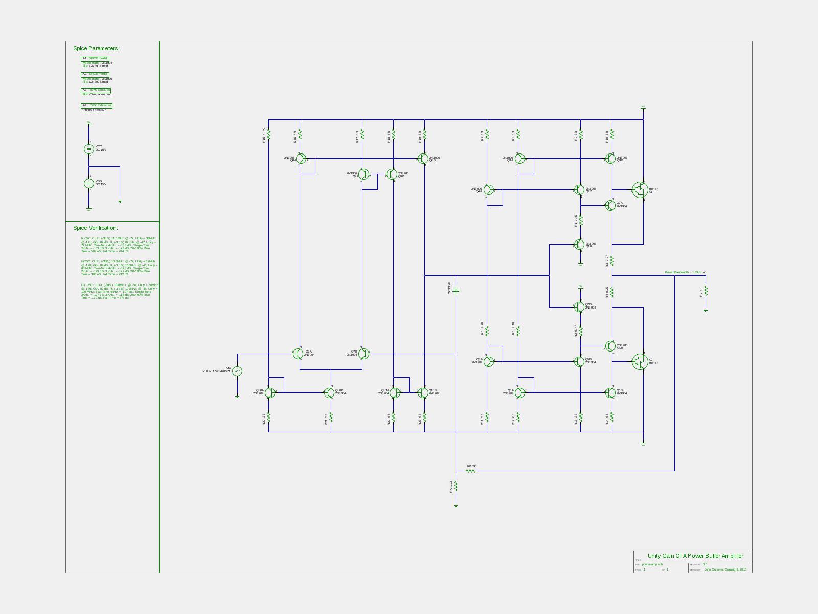
Figure V, (1600X1200),(3200X2400), is the schematic of the preceding design, with complementary Darlington transistors replaced with MOS FET power transistors, in the fet-power-amp/ directory. The sub-directories, (DC/, Zi/, Zo/, distortion/, distortion/two-tone, noload/, openloop/, openloop/distortion/, openloop/distortion/two-tone, transient/,) contain the analysis. The 25C second order distortion at 2KHz. is 0.17% = -55.2 dB, and the two tone distortion, (6KHz., and 8KHz.) at 4KHz. is 0.037% = -68.5 dB, (both relative to maximum output = 7 V RMS into 4 Ohms.) The gain varies from 0.9 to 1.0 over military temperature range, and the -3 dB frequency response is over 100MHz., (unity gain is over 400 MHz.,) to accommodate inclusion in the closed loop of a high quality audio operational amplifier front end, (as used in the Direct Coupled Stereo Headphone Amplifier project with appropriate frequency compensation,) and reduce the distortion levels to acceptable levels of the design requirements. The total cost of the semiconductors in the circuit is under US $7, but all the transistors, (excepting the MOS FET power transistors output drivers,) are matched pairs, (meaning available packages are SOT, only.) It is interesting to note the higher second order distortion of this design over the equivalent bipolar design-mention will be made later.
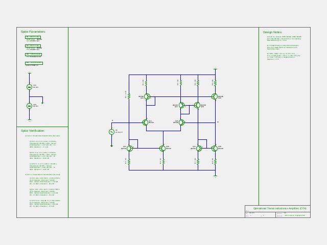
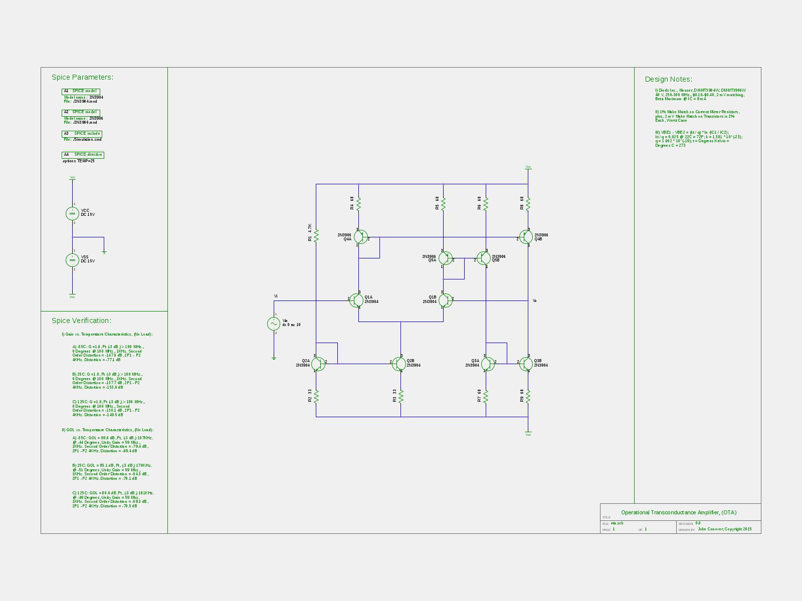
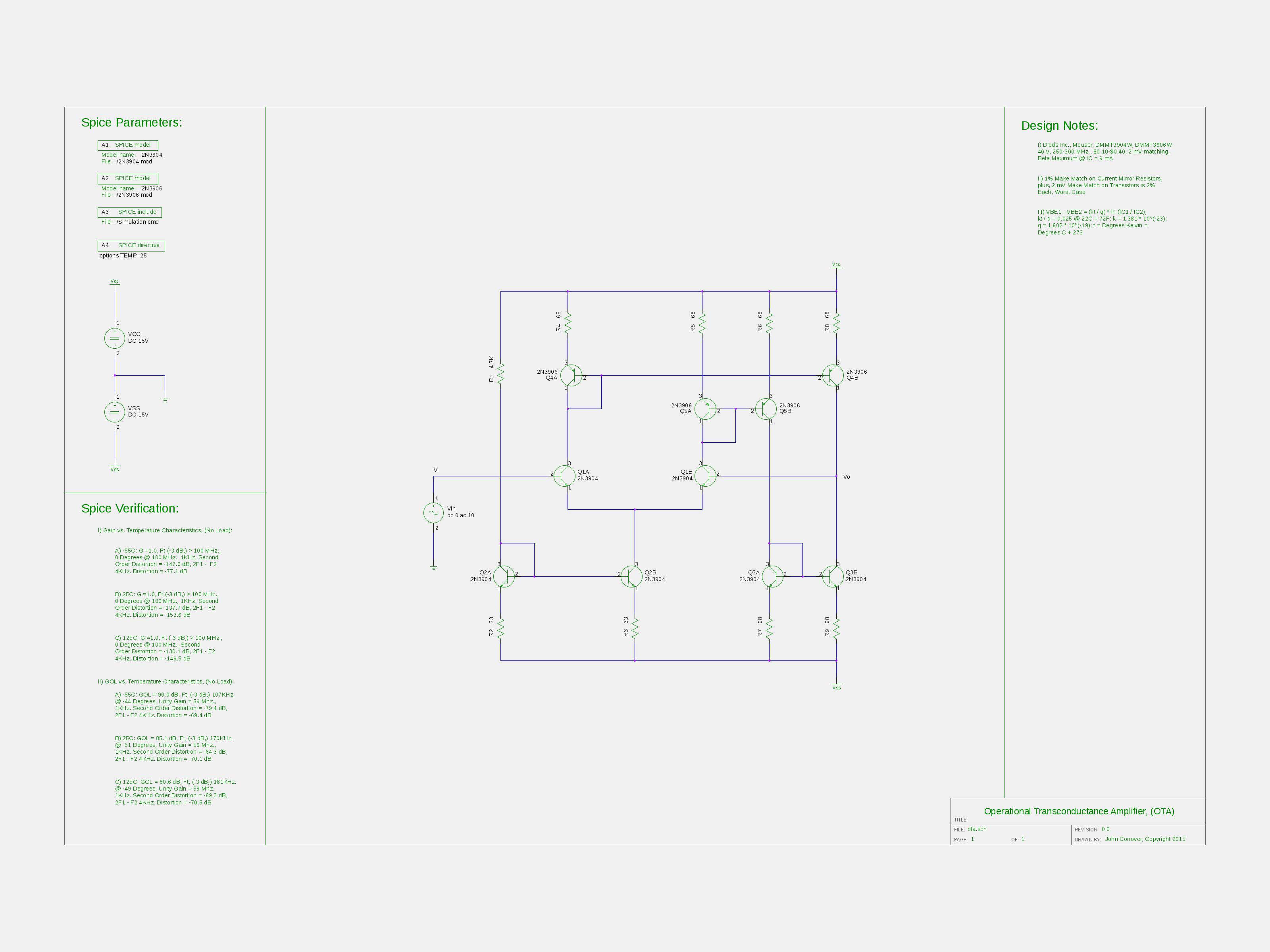
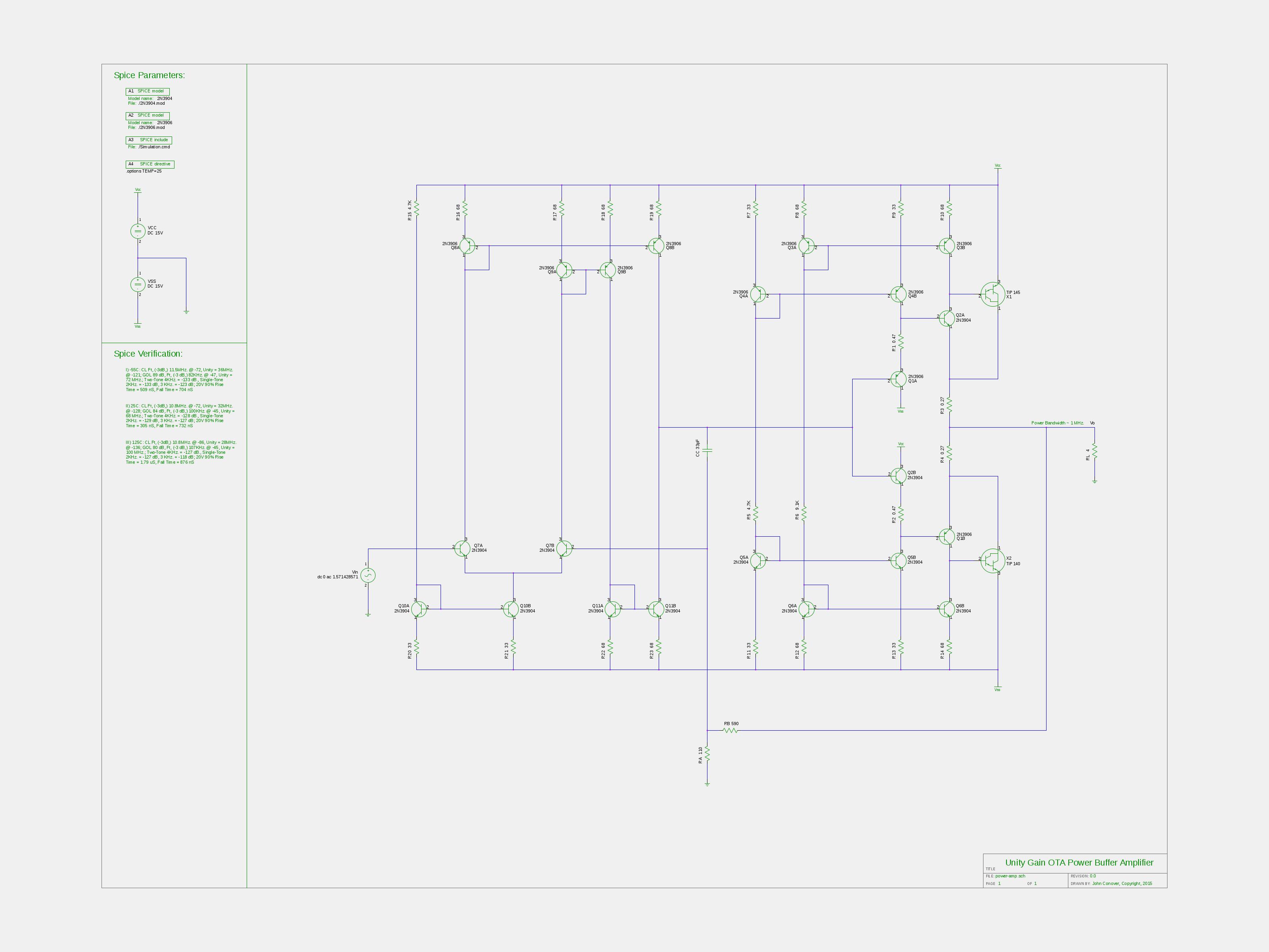
Figure VI, (1600X1200),(3200X2400), is the schematic of the discreet bipolar Operational Transconductance Amplifier, (OTA,) in the ota/ directory. The sub-directories, (distortion/, distortion/two-tone, openloop/, openloop/distortion, openloop/distortion/two-tone,) contain the analysis. The no-load open loop gain of the OTA amplifier is about 10,000 = 80 dB at 25C, with a -3dB bandwidth of about 200 KHz., and a unity gain of slightly over 100 MHz. The amplifier is not unity gain stable, (this will be exploited, below, when the output of the OTA is connected to its inverting input through a capacitor-making the OTA an integrator-to provide the dominant pole frequency compensation for the combined circuits in the ota/ and power-amp/ directories when the ota-power-amp/ directory is analyzed.) The 25C second order no load distortion at 2KHz. is 0.000013% = -137.7 dB, and the two tone distortion, (6KHz., and 8KHz.) at 4KHz. is 0.000002% = -153.6 dB, (both relative to maximum output = 7 V RMS.) Remember that these numbers are for no load conditions on the OTA output, and will change when connected to the high impedance input of the unity gain buffer amplifier, (note that we are depending on this to provide frequency compensation for high frequency stability of the combined amplifiers.) The total cost of the semiconductors in the circuit is under US $3, but all the transistors are matched pairs, (meaning available packages are SOT, only.)
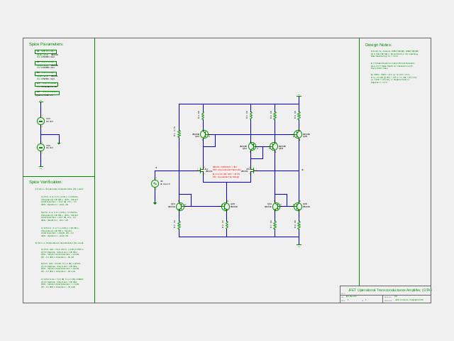
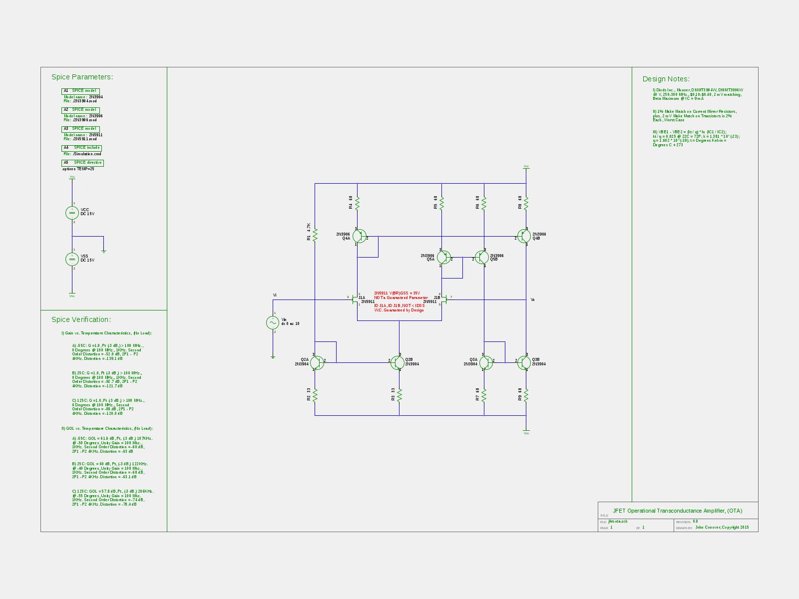
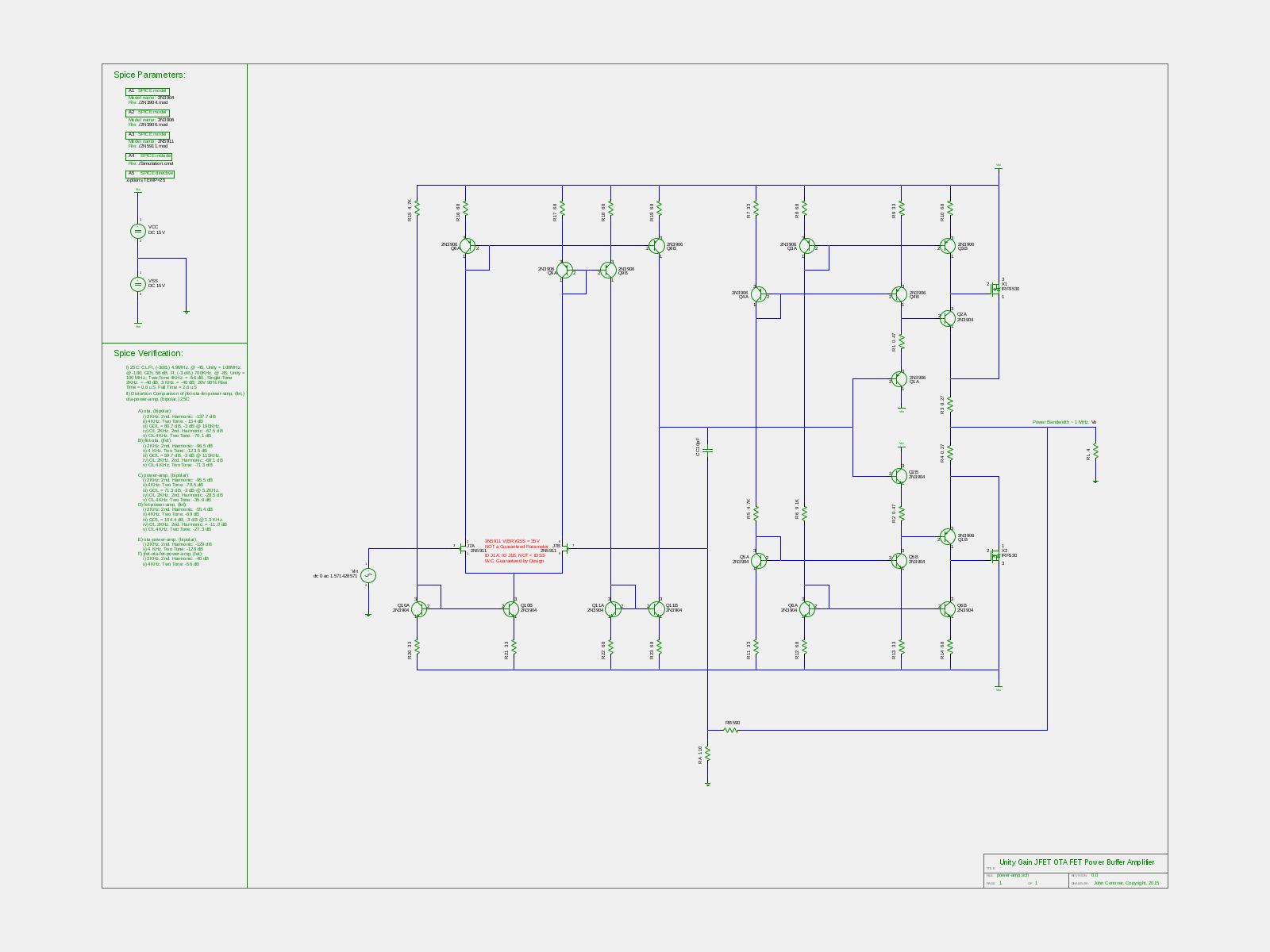
Figure VII, (1600X1200),(3200X2400), is the schematic of the preceding OTA design, with the differential input transistors replaced with matched JFET transistors, in the jfet-ota/ directory. The sub-directories, (distortion/, distortion/two-tone, openloop/, openloop/distortion, openloop/distortion/two-tone,) contain the analysis. The no-load open loop gain of the OTA amplifier is about 1,000 = 60 dB at 25C, with a -3dB bandwidth of about 95 KHz., and a unity gain of about 100 MHz. The amplifier is not unity gain stable, (this will be exploited, for reasoning similar to the preceding OTA design,) The 25C second order no load distortion at 2KHz. is 0.0016% = -96.1 dB, and the two tone distortion, (6KHz., and 8KHz.) at 4KHz. is 0.000067% = -123.5 dB, (both relative to maximum output = 7 V RMS.) Remember that these numbers are for no load conditions on the OTA output, and will change when connected to the high impedance input of the unity gain buffer amplifier. The total cost of the semiconductors in the circuit is under US $4, but all the transistors are matched pairs, (meaning available packages are SOT, only.)
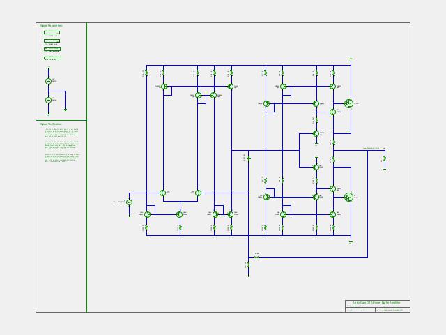
Figure VIII, (1600X1200),(3200X2400), is the schematic of the combined bipolar OTA amplifier in the ota/ directory, with the bipolar unity gain power amplifier in the power-amp/ directory, in the ota-power-amp/ directory. The sub-directories, (distortion/, distortion/two-tone, openloop/, openloop/distortion/, openloop/distortion/two-tone, transient/,) contain the analysis. The 25C second order distortion at 2KHz. is 0.000034% = -129.2 dB, and the two tone distortion, (6KHz., and 8KHz.) at 4KHz. is 0.000035% = -128.5 dB, (both relative to maximum output = 7 V RMS into 4 Ohms,) over military temperature range, and the -3 dB frequency response is almost 10MHz., (unity gain is almost 50 MHz.) The total cost of the semiconductors in the circuit is under US $10, (per channel,) but all the transistors, (excepting the Darlington output drivers,) are matched pairs, (meaning available packages are SOT, only.) Note that the design requirments, over military temperature range, have been met, and distortion products in the 2KHz. to 5KHz. frequency range are an order of magnitude below the minimum threshold of human hearing, (MTH.)
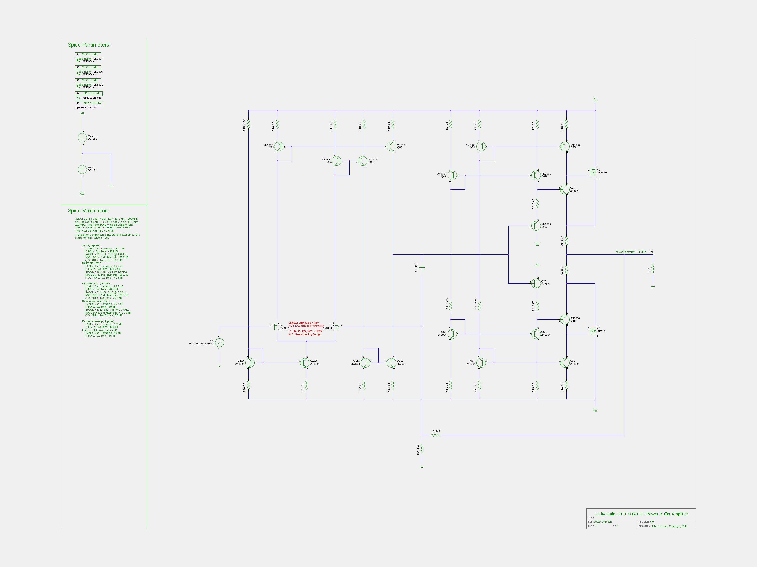
Figure IX, (1600X1200),(3200X2400), is the schematic of the combined JFET input OTA amplifier in the jfet-ota/ directory, with the power FET unity gain power amplifier in the fet-power-amp/ directory, in the jfet-ota-fet-power-amp/ directory. The sub-directories, (distortion/, distortion/two-tone, openloop/, openloop/distortion/, openloop/distortion/two-tone, transient/,) contain the analysis. The 25C second order distortion at 2KHz. is 1.0% = -40 dB, and the two tone distortion, (6KHz., and 8KHz.) at 4KHz. is 0.16% = -56.0 dB, (both relative to maximum output = 7 V RMS into 4 Ohms,) over military temperature range, and the -3 dB frequency response is about 6MHz., (unity gain is about 100 MHz.) The total cost of the semiconductors in the circuit is under US $15, (per channel,) but all the transistors, (excepting the power FETs,) are matched pairs, (meaning available packages are SOT, only.) Note that this design did not meet the design requirements-the second order distortion at 2KHz. is only -40 dB, below 100 dB = 0 dBFS, (which should correspond to 100 dB SPL.) DiscussionNote the amplifier circuit topology philosophy. Sections of the amplifier that have high distortion, (high current output driver transistors, and low level differential signal input transistors, in that order,) should have local nested negative feedback loops, and a negative feedback loop around the entire amplifier chain to lower distortion to acceptable levels. The input signal is converted to a current, immediately, and the current signal amplified, as linearly as possible. The current signal drives a high impedance unity closed loop gain power amplifier, which is where the voltage gain occurs. The quiescent current in the unity gain power amplifier is sensed by external transistors that are not subject to thermal management issues of the high current output driver transistors; lack of quiescent current control in the driver transistors is a source of distortion over the military temperature range. Finally, a relatively simple frequency compensation scheme is available at the high impedance point where the OTA amplifier is connected to the unity gain power buffer. As a final note, although the FET transistor designs did not meet the design requirements, many consider the high second order distortion "pleasing", (specifically, rock, jazz, and blues musicians.) A similar statement can be made for vacuum tube designs. The effect is an apparent increase in dynamic range and loudness without high SPL levels. However, many classical music prodigies, (particularly the gifted young, with good trained ears,) do not like any distortion to be audible. The amplifiers in the jfet-ota-fet-power-amp/ and ota-power-amp/ directories can have a distortion "tweek" added: a resistor, (possibly variable,) from the output of the OTA amplifier to ground. Smaller resistor means lowering the open loop gain of the amplifier, which means less negative feedback, which means more distortion. And, it can be made frequency sensitive with reactive components. LicenseA license is hereby granted to reproduce this software for personal, non-commercial use. THIS PROGRAM IS PROVIDED "AS IS". THE AUTHOR PROVIDES NO WARRANTIES WHATSOEVER, EXPRESSED OR IMPLIED, INCLUDING WARRANTIES OF MERCHANTABILITY, TITLE, OR FITNESS FOR ANY PARTICULAR PURPOSE. THE AUTHOR DOES NOT WARRANT THAT USE OF THIS PROGRAM DOES NOT INFRINGE THE INTELLECTUAL PROPERTY RIGHTS OF ANY THIRD PARTY IN ANY COUNTRY. So there. Copyright © 1992-2015, John Conover, All Rights Reserved. Comments and/or problem reports should be addressed to:
|
Home | John | Connie | Publications | Software | Correspondence | NtropiX | NdustriX | NformatiX | NdeX | Thanks